This is printing a lithograph on a solid, flat overside or a metal plate. The image parts are designed using a greasy material like pencil, lacquer, crayon, or tusche. The flat surface transfers ink to the paper in areas that mirror the pattern.
To separate the grease-receiving image areas and water-receptive non-printing areas, a mixture of nitric acid and gum arabic, is put on the surface. This creates a resistadhesion in lithography because grease and water do not mix.
Types of lithography methods are:
X-ray lithography
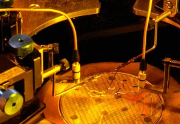
Electronic manufacturers use this process to remove some parts of a film selectively. It uses an x-ray to send geometric patterns from a mask to a chemical photoresist on the surface. This is followed by chemical treatments that inscribe the pattern into the material under the photoresist. The source of x-ray starts with an electron beam and is then changed to an x-ray beam with a synchrotron.
Advantages of x-ray lithography
Process is fast.It is not affected by an organic fault in the mask.There is a decrease in reflection and diffraction effects.Disadvantages
X-ray mask fabrication is not easy.Shadow printing style.This lithography method is commonly used in computer chips and other electrical devices.Offset lithography
This method involves printing the design on the middle surface before the last sheet. The plate does not have contact with the paper, and it maintains the quality of the plate. With this lithography procedure, the design is reversed two times and shows on the final sheet similar to that on the hard surface.
Electron beam lithography
This form of lithography is the transfer of a pattern to the surface of the substrate, using a nEBL3 Selective e -Beam to scan a resist.
The electron beam is concentrated, and the resist’s exposed or non-exposed areas are selectively removed. The exposed areas are processed for etching, and the other is protected.
E-beam resists are made for electron beam and deep UV applications to produce highly integrated circuits, mainly manufacturing masks.
You can get 100 to 500nm structures on masks and wafers, with f 200 and 500nm thickness values. An advantage of an e-beam is that the wavelength of an accelerated electron is short.
Extreme extra violet lithography
This major chip printing method uses extreme ultraviolet wavelengths, about 2%FWHM bandwidth estimated to be about 13.5nm.
This advanced technology uses one mask exposure rather than multiexposure. EUV lithography tools use a plasma source to produce 13.5 nm photons. The collector gathers light from the plasma utilizing an optical element.
The collector is focused on a group of shaping optics called illumination optics, which comprises multilayer-coated normal incidence and grazing incidence mirrors.
The mirrored image of the mask goes into a projection optic, which consists of six multilayer mirrors or more via demagnification. The last image is then concentrated into silicon coated with a photoresist.
Conclusion
Artists still prefer the method of using hard surfaces for lithography. Commercial lithography through offset produces good quality materials at high speed in plate making.
0


Sign in to leave a comment.