In the realm of printed circuit board assembly services, Ball Grid Array (BGA) technology stands out as a pivotal advancement, enabling the development of compact, high-performance electronic devices. At A2ZEMS Electronics , we pride ourselves on delivering top-tier PCB assembly services, including expertise in BGA technology. This guide delves into the intricacies of BGA, its advantages, challenges, and the meticulous processes involved in its implementation.
Understanding Ball Grid Array (BGA) Technology
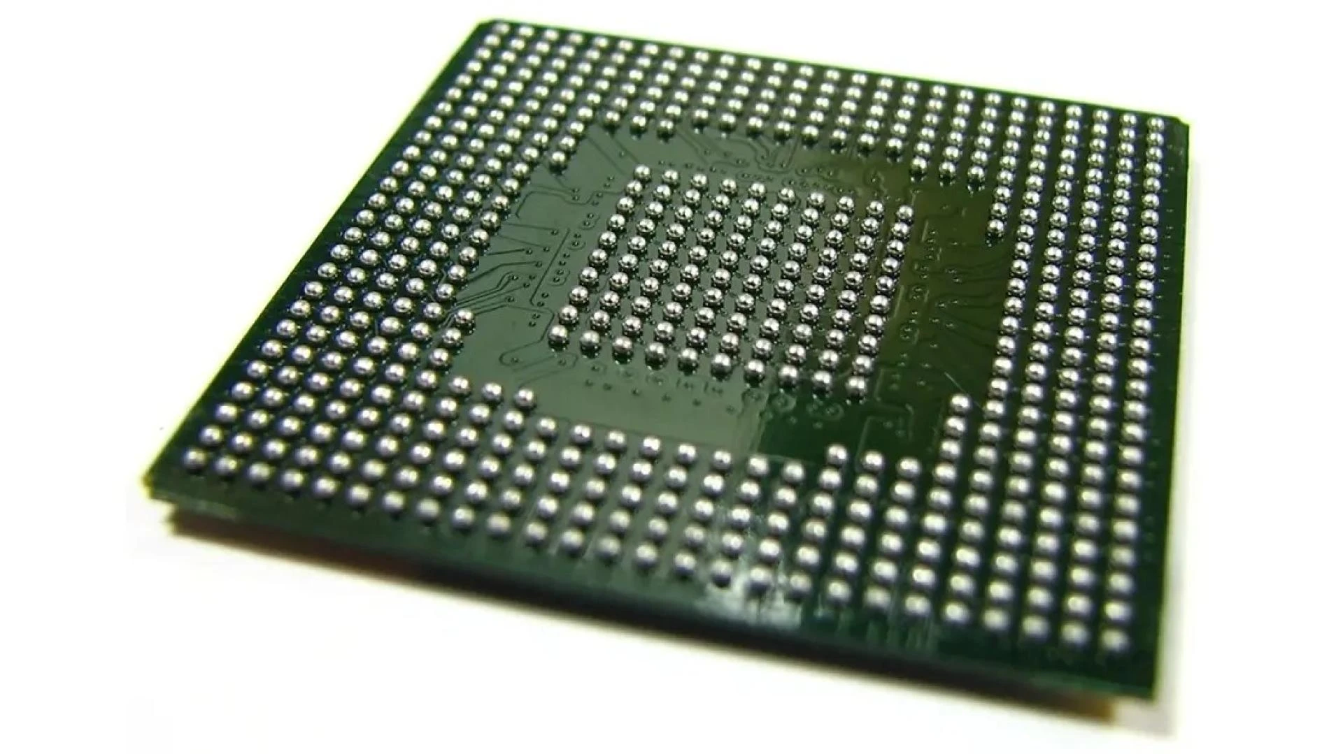
Ball Grid Array (BGA) is a surface-mount packaging method used for integrated circuits. Unlike traditional packages that utilize pins or leads, BGA employs an array of solder balls on the underside of the component to establish electrical connections with the printed circuit board (PCB). This design facilitates higher interconnection density and enhances the electrical and thermal performance of the assembled device.
Structure of a BGA Package
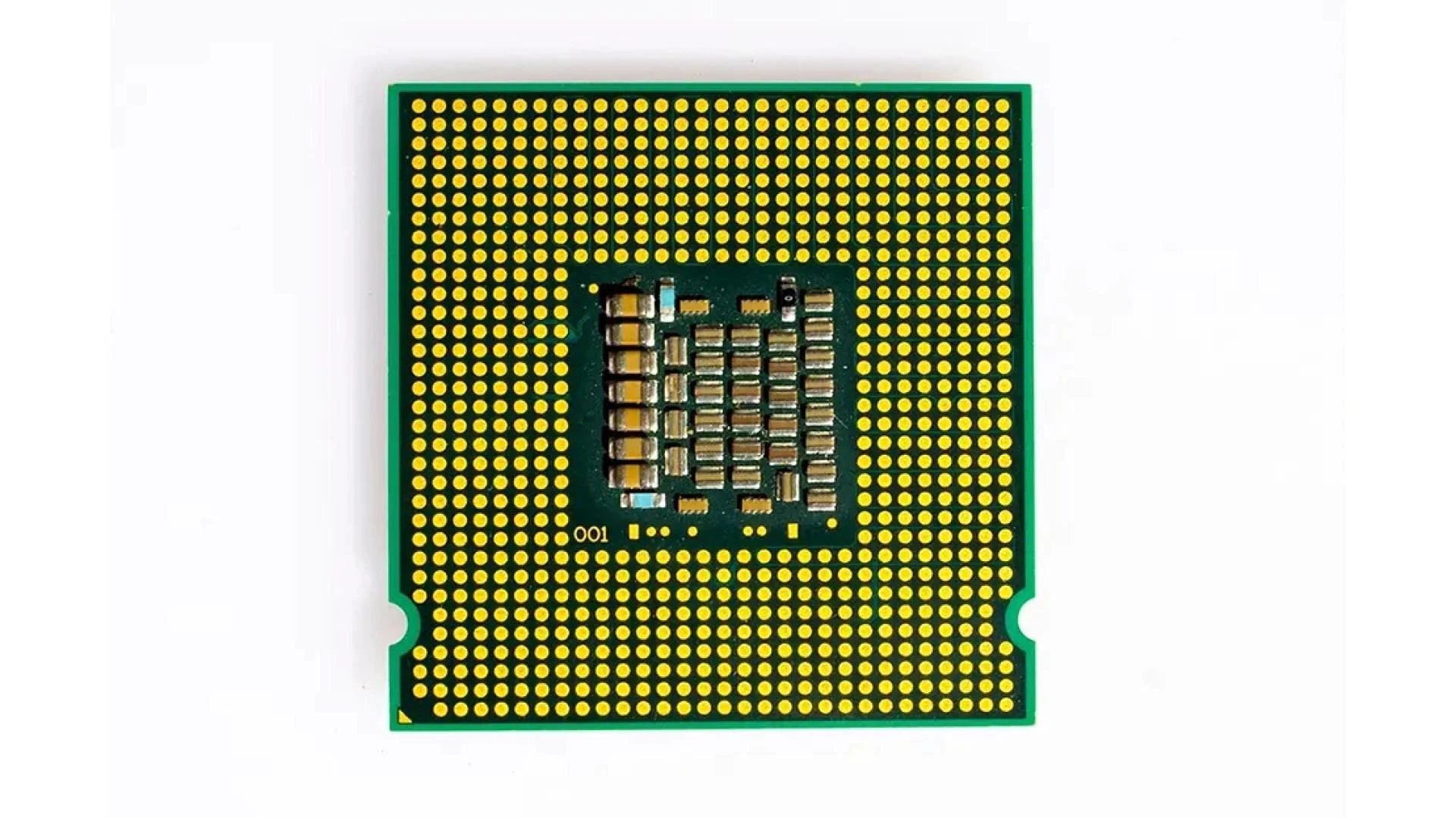
A standard BGA package comprises:
- Integrated Circuit (IC) Die: The semiconductor component that performs the device's functions.
- Substrate: A laminated material that provides mechanical support and electrical pathways between the die and the solder balls.
- Solder Balls: Spherical solder connections arranged in a grid pattern on the package's underside.
- Encapsulation Material: Protective covering that shields the IC die and internal connections from environmental factors.
Advantages of BGA in PCB Assembly
Implementing BGA technology in printed circuit assembly services offers several notable benefits:
High-Density Interconnections
BGA packages utilize the entire bottom surface for solder balls, allowing for a greater number of connections compared to perimeter-limited packages. This design is particularly advantageous for devices requiring numerous I/O connections without increasing the package size.
Enhanced Electrical Performance
The short, uniform connection paths in BGA packages reduce inductance and resistance, leading to improved signal integrity and performance at high frequencies. This characteristic is essential for modern high-speed electronic applications.
Superior Thermal Management
The solder balls in BGA packages serve as effective conduits for heat dissipation, transferring thermal energy from the IC die to the PCB. This efficient heat transfer minimizes the risk of overheating and enhances the reliability of the device.
Interesting Reads: PCB Assembly vs. PCB Fabrication: What to Choose for Your Next Electronics Project
Challenges in BGA Assembly
Despite its advantages, BGA technology presents specific challenges in the PCB assembly services process:
Inspection Difficulties
Post-soldering inspection of BGA joints is complex due to their concealed nature beneath the package. Traditional visual inspection methods are inadequate, necessitating advanced techniques such as Automated X-ray Inspection (AXI) to detect defects like voids, misalignments, or solder bridges.
Rework Complexity
Addressing defects in BGA assemblies requires precise equipment and expertise. The rework process involves carefully heating the specific component to detach it without affecting neighboring areas, demanding meticulous control to prevent damage to the PCB or adjacent components.
BGA Assembly Process at A2ZEMS
At A2ZEMS Electronics, we offer comprehensive turnkey PCB assembly solutions, encompassing the entire BGA assembly process with precision and quality assurance. Our approach includes:
- Design for Manufacturability (DFM) Review: Assessing PCB designs to ensure compatibility with BGA assembly, focusing on pad design, thermal considerations, and manufacturability.
- Solder Paste Application: Utilizing high-precision stencils and printers to apply solder paste accurately to the PCB pads designated for BGA components.
- Component Placement: Employing advanced pick-and-place machines to position BGA components with high accuracy, ensuring proper alignment with the PCB pads.
- Reflow Soldering: Carefully controlling the temperature profile during reflow soldering to achieve reliable solder joints without inducing thermal stress.
- Inspection and Quality Control: Implementing rigorous inspection protocols, including AXI, to verify the integrity of BGA solder joints and ensure the highest quality standards.
Applications of BGA Technology
BGA technology is integral to various sectors requiring compact, high-performance electronic solutions. At A2ZEMS Electronics, we provide quick turn PCB assembly services for industries such as:
- Consumer Electronics: Smartphones, tablets, and other portable devices.
- Automotive Electronics: Advanced driver-assistance systems (ADAS) and infotainment systems.
- Medical Devices: Diagnostic equipment and wearable health monitors.
- Telecommunications: Networking hardware and communication devices.
Interesting Reads : How to Select the Right Electronic Components for Your Design
End Analysis
Ball Grid Array (BGA) technology is a cornerstone in modern PCB assembly services, offering unparalleled advantages in interconnection density, electrical performance, and thermal management. At A2ZEMS Electronics, we are committed to delivering exceptional printed circuit board assembly services, leveraging our expertise in BGA technology to meet the evolving demands of the electronics industry.
Whether you're seeking PCB assembly near me or specialized solutions like fast turn printed circuit board assembly, our team is dedicated to providing quality, efficiency, and reliability in every project.
For more information on our PCB assembly services or to discuss your specific project requirements, please visit our website at A2ZEMS Electronics.
FAQ: Ball Grid Array (BGA) Technology in PCB Assembly
What is BGA in PCB?
BGA (Ball Grid Array) is a surface-mount packaging technology where solder balls form electrical connections between the component and the PCB.
What is a BGA Package?
A BGA package is an IC package using solder balls arranged in a grid pattern for reliable connectivity and improved performance.
What are the Different BGA Package Types?
Common types include PBGA (Plastic), CBGA (Ceramic), TBGA (Tape), µBGA (Micro), and FCBGA (Flip-Chip), each designed for specific applications.
What are BGA Components?
BGA components include microprocessors, GPUs, memory chips, FPGAs, ASICs, and power management ICs, used in various high-performance electronics.
What is the Full Form of BGA?
BGA stands for Ball Grid Array, referring to the arrangement of solder balls on the bottom of the package.
What Are the Common BGA Package Sizes?
Sizes vary with pitch (0.4mm–1.27mm), ball count (50–1000+), and dimensions (5mm × 5mm to 50mm × 50mm), depending on application.
What is the Difference Between BGA and FPGA?
BGA is a packaging technology, while FPGA is a programmable chip that may come in a BGA package for better performance.


Sign in to leave a comment.