P-N junction is formed by joining n-type and p-type semiconductor materials, which is a two terminal device that allows electric current in one direction and blocks electric current in another direction.
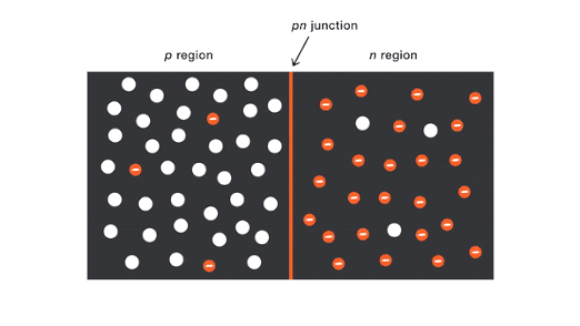
On a silicon wafer, different doping processes are used to form an N-type semiconductor on one side and a P-type semiconductor on the other side. We call the area near the interface of the two semiconductors a PN junction.
1 PN Junction Characteristic
1.1 Unidirectional Conductivity
(1) The PN junction is turned on when the forward voltage is applied.
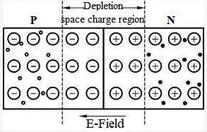
If the positive pole of the power supply is connected to the P area and the negative pole is connected to the N area, a part of the applied forward voltage is in the PN junction area, at this time, the PN junction is in a forward bias. The current flows from the P to the N, and the holes and electrons move to the interface, which narrows the space charge area. In addition, the current can pass smoothly. Its direction is opposite to the direction of the electric field in the PN junction, which weakens the internal electric field. As a result, the resistance of the internal electric field to the diffusion movement of the multitons weakens, and the diffusion current increases. The diffusion current is much larger than the drift current, and the influence of the drift current can be ignored, and the PN junction is in low resistance.
(2) PN junction is cut off when reverse voltage is applied.
If the positive pole of the power supply is connected to the N zone, the negative pole is connected to the P zone, and a part of the applied reverse voltage applies in the PN junction zone, and it is in reverse bias. Then the holes and electrons move away from the interface, which widens the space charge area, and the current cannot flow. The direction is the same as the direction of the electric field in the PN junction, which strengthens the internal electric field. The resistance of the internal electric field to the multiton diffusion movement is enhanced, and the diffusion current is greatly reduced. At this time, the drift current formed by the minority carriers in the PN junction region under the action of the internal electric field is greater than the diffusion current. The diffusion current can be ignored, and the PN junction exhibits high resistance.
1.2 Reverse Breakdown
When a reverse voltage is applied to the PN junction, the space charge region becomes wider and the electric field in the region strengthens. When the reverse voltage increases to a certain level, the reverse current will suddenly increase. If the external circuit cannot limit the current, the current will be so large that it will burn the PN junction. At this time, it is called the breakdown voltage. There are two basic breakdown ways, namely tunnel breakdown (also called Zener breakdown) and avalanche breakdown. The former has a breakdown voltage of less than 6V and has a negative temperature coefficient, and the latter has a breakdown voltage of greater than 6V and a positive temperature coefficient.
1.3 Volt-Ampere Characteristics
The volt-ampere characteristics of the PN junction are shown in the figure, which visually shows the unidirectional conductivity.
The volt-ampere characteristic shows by:
Where iD is the current passing through the PN junction, VD is the applied voltage at both ends of the PN junction, and VT is the voltage equivalent of temperature.
1.4 Capacitance Characteristics
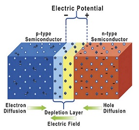
When a reverse voltage is applied to the PN junction, the positive and negative charges in the space charge region constitute a capacitive device. Its capacitance changes with the applied voltage, mainly including barrier capacitance (CB) and diffusion capacitance (CD). Both of them are non-linear capacitors.
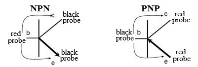
2 Transistor NPN-Type and PNP-Type Junctions
Transistors are one of the basic building blocks of modern electronics. In the diode tutorials we saw that simple diodes are made up from two pieces of semiconductor material to form a simple pn-junction. While the transistor is a three terminal solid state device which is formed by connecting two diodes back to back. Hence it has got two PN junctions.
Transistor Working State
The transistor works like an electronic switch. It can turn a current ON and OFF. The basic idea behind a transistor is that it lets you control the flow of current through one channel by varying the intensity of a much smaller current that's flowing through a second channel.
1) Cut-off State (C): The base current is zero.
2) Amplified State (A): The transmitter junction is forward biased (that is, the voltage direction is P->N), and the collector junction is reverse biased.
3) Saturation State (S): Both the emitter junction and the collector junction are forward biased.
* Working State
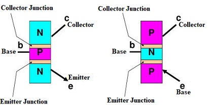
1) NPN-Type Transistor
Vb<Ve (C)
Vc>Vb>Ve (A)
Vb>Ve Vb>Vc (S)
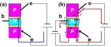
2) PNP-Type Transistor
Vb>Ve (C)
Vc<Vb<Ve (A)
Vb<Ve Vb<Vc (S)
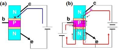
Figure (a), when there is no voltage input at b of the NPN transistor, no current flows between c and e, and the triode is in the cut-off state.
Figure (b), when a positive voltage is input to b of the NPN transistor, the negative electrons in the N region of e are attracted by the positrons of P region in b. Due to the effect of the power plant, and they rush (diffuse) to the base region, however, only part of the negative electrons collide with the positive electrons (recombination) to generate the base current, and the other part of the negative electrons gather near the collector junction. The negative electrons gathered in the collector junction pass through (drift) the collector junction due to the action of the electric field. After reaching the collector area, it collides with the positrons gathered in c (N-type semiconductor terminal) to generate a collector current.
It can be seen from this that the greater the base current, the greater the collector current. That is, when a small current is input to the collector, a large current can be obtained by the collector, and now the transistor is in an amplified state.
It should be noted that when the base current reaches a certain level, the collector current no longer rises. At this time, the transistor loses its current amplification effect, and the voltage between the collector and the emitter is very small. The collector and emitter are equivalent to the on-state of the switch. At this moment, the transistor is in a saturated state.
Because of words limit, you can read the full note from What is a PN Junction Diode?