
Navigating the Global Electron-Beam Writer Market: Strategic Trends and Commercial Opportunities Through 2032
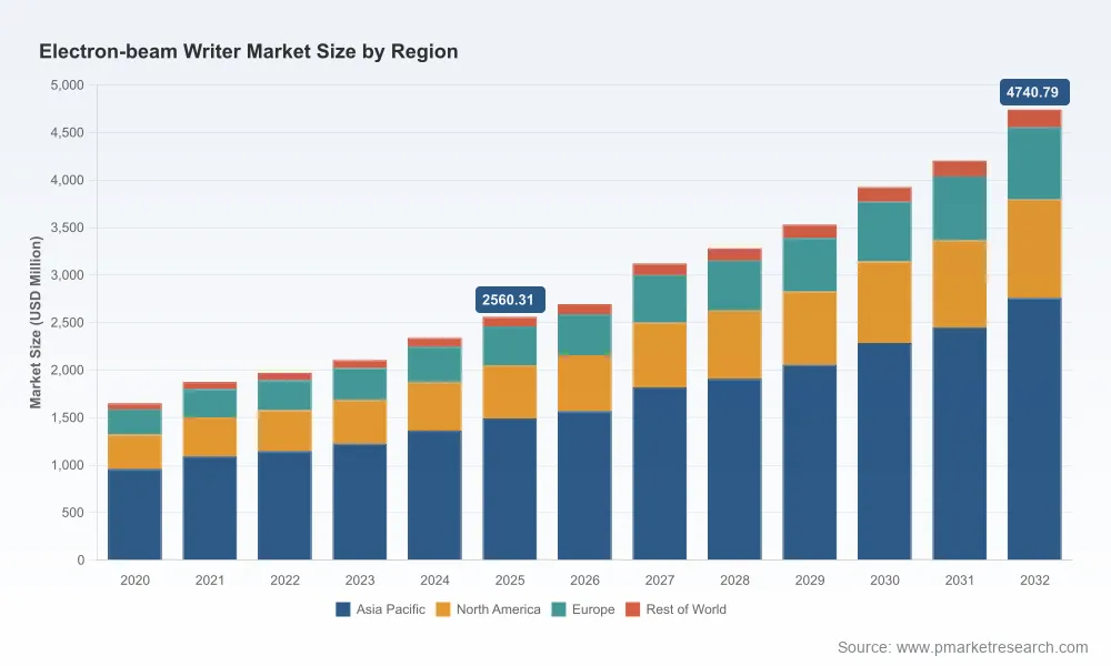
The worldwide electron-beam writer market has entered a phase of sustained expansion, driven by the escalating complexity of semiconductor patterning and the growing demand for high-resolution lithography across both mature and advanced nodes. Valued at approximately $2.56 billion in 2025, the market is projected to surpass $4.7 billion by 2032, reflecting a compound annual growth rate of 9.2 percent over the forecast period. This trajectory underscores a structural shift: electron-beam lithography is no longer confined to academic laboratories or niche prototyping environments. It has become an indispensable enabler for photomask manufacturing, direct-write applications, and specialized research initiatives that require feature sizes unattainable through conventional optical or EUV lithography alone.
Despite the robust growth outlook, the industry faces several critical inflection points. First, throughput remains a persistent bottleneck. Electron-beam systems inherently operate on a serial or semi-parallel basis, making them economically uncompetitive for high-volume manufacturing at advanced nodes. This limitation forces manufacturers to carefully balance resolution, throughput, and cost when selecting patterning strategies for production lines. Second, geographic and regulatory fragmentation introduces complexity into technology deployment and procurement. Export controls targeting advanced semiconductor manufacturing equipment, particularly those involving U.S. export administration regulations and allied restrictions on lithography technologies, have reshaped supply chain planning and limited market accessibility in certain regions. These regulatory dynamics require equipment suppliers and end-users to navigate licensing requirements, end-use restrictions, and evolving compliance frameworks that can delay product introductions or constrain cross-border collaborations. Third, the industry must reconcile the dual demands of mask-making productivity and direct-write flexibility. Traditional mask writers prioritize throughput for complex reticle patterns, while direct-write systems emphasize precision for low-volume, highly customized designs. Bridging these use cases without compromising performance or economic viability remains a defining challenge for equipment developers and semiconductor fabs alike.
Core Drivers Shaping the Electron-Beam Writer Landscape
Technological Innovation and Architecture Evolution
The most transformative force in the electron-beam writer market is the ongoing evolution from single-beam and variable-shaped beam architectures toward multi-beam and multi-column configurations. Multi-beam systems leverage thousands of programmable beams to parallelize patterning, effectively decoupling write times from pattern complexity for photomask production. This architectural shift has enabled manufacturers to address advanced nodes ranging from 28nm down to 5nm and beyond, particularly for EUV mask fabrication and nanoimprint lithography template production. By reducing the sensitivity of throughput to pattern density, multi-beam writers are expanding the economic viability of electron-beam lithography in high-value photomask workflows. At the same time, multi-column direct-write platforms are emerging for 300mm wafer and panel-level applications, targeting advanced packaging, AI accelerator chips, photonics, MEMS, and compound semiconductors. These systems combine high depth of focus with maskless patterning capabilities, offering manufacturers a flexible alternative for rapid prototyping and low-to-medium volume production where traditional mask-based approaches carry prohibitive cost or cycle-time penalties.
Parallel to hardware innovation, software and computational lithography advancements are playing an increasingly critical role. Advanced pattern fracturing, dose correction algorithms, and automated beam calibration routines are improving throughput and defectivity across diverse substrate sizes, including 200mm and 300mm wafers as well as specialized panels. These software-driven improvements help close the performance gap between electron-beam lithography and higher-throughput optical methods, enabling more seamless integration into existing fab workflows. For research institutions and small-to-medium enterprises, system configurations that support mix-and-match approaches—such as combining electron-beam lithography with laser or ion beam processing—provide additional flexibility for exploratory device development and rapid iteration.
Policy and Regulatory Dynamics
Regulatory developments have become a defining factor in market access, procurement planning, and technology roadmapping. Export controls targeting certain electron-beam lithography equipment and related semiconductor manufacturing items require licenses for exports, reexports, or transfers to specific destinations when the equipment is used in the development or production of advanced-node integrated circuits. These controls, enforced through U.S. export administration regulations and reinforced by allied restrictions on advanced lithography technologies, introduce compliance complexity into global supply chains. For equipment vendors, this means enhanced due diligence, customer qualification processes, and region-specific commercial strategies. For end-users, especially those operating across multiple jurisdictions, it necessitates careful assessment of procurement timing, alternative sourcing options, and potential impacts on product development cycles.
At the same time, regulatory scrutiny is driving a degree of regionalization in technology deployment. Semiconductor ecosystems in North America, Europe, Japan, and parts of Asia are investing in domestic or allied supply chains to reduce dependency on restricted pathways. This shift creates both opportunities and constraints. On one hand, localized production and development can stimulate demand for domestically supported electron-beam writer systems, particularly in research, mask-making, and specialized manufacturing segments aligned with national strategic priorities. On the other hand, restricted access to certain advanced-node fabrication capabilities can limit the addressable market for direct-write and photomask applications that depend on cutting-edge process integration. Companies that proactively align their product portfolios, compliance frameworks, and regional partnerships with these regulatory realities are better positioned to navigate the evolving landscape.
Demand-Side Shifts in Photomask Manufacturing and Advanced Applications
Photomask manufacturing remains the dominant application area for electron-beam writers, reflecting the central role of high-precision reticle production in advanced semiconductor fabrication. As design rules shrink and mask complexity increases, the demand for defect-free, high-resolution mask writing continues to grow. Multi-beam mask writers have transitioned into production use for advanced photomasks, delivering predictable write performance for EUV masks and nanoimprint templates. This transition is particularly significant because it addresses one of the longstanding limitations of electron-beam lithography: throughput variability driven by pattern complexity. By stabilizing write times and improving productivity, these systems support the expanding photomask requirements of leading-edge chip development and production.
Beyond traditional photomasks, demand is broadening into specialized and emerging applications. Direct-write lithography is gaining traction for advanced packaging, where heterogeneous integration, chiplet architectures, and high-bandwidth interconnects require precise, customized patterning that does not always justify full mask sets. AI and high-performance computing chips, photonics-based interconnects, MEMS devices, and compound semiconductor components are driving interest in flexible, high-resolution patterning solutions. Research and development activities in quantum technologies, nanophotonics, and novel device architectures further contribute to sustained demand for electron-beam lithography tools that can handle sub-10nm feature sizes with high accuracy. For many of these applications, the value proposition lies not in competing with high-volume optical lithography but in enabling rapid iteration, low-volume production, and design-specific customization that mask-based workflows cannot easily support.
Supply Chain and Cost Structure Considerations
Cost dynamics in the electron-beam writer market are being shaped by a combination of semiconductor equipment sourcing complexity, substrate diversity, and the economics of maskless versus mask-based workflows. While electron-beam systems command premium pricing due to their resolution and flexibility, total cost of ownership considerations increasingly influence purchasing decisions. For research institutions and small-scale production environments, systems that balance resolution with automated loading, user-friendly software, and relatively straightforward maintenance can reduce operational friction and accelerate time-to-pattern. For mask-making facilities, investment decisions are driven by throughput, yield, and the ability to handle evolving mask specifications for EUV and advanced optical nodes.
Supply chain considerations also play a role in vendor selection and deployment timelines. Regional concentration of advanced semiconductor manufacturing, combined with export control frameworks and allied restrictions, has prompted organizations to diversify sourcing strategies and strengthen relationships with equipment suppliers that can provide localized support, service networks, and compliance guidance. In parallel, the emergence of production-oriented electron-beam systems for direct wafer writing reflects a broader shift toward reducing reliance on mask cycles for certain applications, which can lower non-recurring engineering costs and shorten development cycles for customized devices. However, these benefits must be weighed against throughput limitations and the need for specialized process integration, particularly when scaling from prototyping to production quantities.
Competitive Landscape and Strategic Positioning
Established Leaders and Differentiated Value Propositions
The electron-beam writer market is characterized by a highly concentrated competitive structure, with a small group of leading vendors capturing the majority of revenue. This concentration reflects the technical complexity of electron-beam lithography, the importance of application-specific optimization, and the long qualification cycles associated with semiconductor equipment. Leading players have carved out distinct strategic positions by aligning their product architectures, target applications, and service models with specific segments of the market.
Specialists in multi-beam mask writing have established a strong presence in photomask production for advanced semiconductor nodes. Their systems are designed to deliver high throughput and precision for complex reticle patterns, with programmable beam arrays that support EUV mask and nanoimprint template fabrication. By focusing on production-oriented mask workflows, these vendors address the critical need for reliable, high-resolution mask writing in leading-edge chip development. Their differentiation stems from proven production track records, system scalability, and deep integration with photomask manufacturing processes.
Other established manufacturers have built comprehensive portfolios spanning research, mask-making, and direct-write applications. Variable-shaped beam systems continue to serve a wide range of use cases, including compound semiconductor processing, photonics, AR/VR development, and low-to-medium volume production on 200mm and 300mm wafers. These systems are valued for their accuracy, flexibility, and ability to support prototyping and specialized manufacturing without the overhead of full mask sets. In parallel, high-performance electron-beam lithography platforms with automated loading and ultra-high resolution capabilities have secured strong positions in research institutions and industry labs, where sub-10nm patterning and experimental device fabrication are paramount.
Pleated Membrane Filter Market
Foundry-adjacent and specialized providers contribute additional dimensions to the competitive landscape. Point-beam systems and electron-beam foundry services support fine-pattern applications such as distributed feedback laser gratings and other photonic structures, combining equipment capabilities with service-oriented business models. Maskless nanofabrication solutions that upgrade scanning electron microscopes or integrate with ion beam and laser processing expand the addressable user base by lowering the barrier to entry for nanolithography in research and rapid prototyping environments.
Emerging Entrants and Strategic Expansion
A notable dynamic in recent market developments is the entry and expansion of newer players focused on production-oriented, maskless direct-write capabilities for wafers and panels. These companies have pursued aggressive commercialization strategies, including significant funding rounds, international sales expansions, and strategic partnerships aimed at accelerating adoption in semiconductor fabrication environments. Recent activity includes multi-column electron-beam lithography platforms targeting 300mm wafer and panel-level applications, with initial production system shipments and partnerships designed to support regional fab ecosystems. Early customers in specialized semiconductor manufacturing have begun integrating these tools for direct maskless patterning, signaling a potential shift in how certain low-to-medium volume, high-customization applications are approached.
These entrants are differentiating themselves by emphasizing high productivity, depth of focus, and applicability to advanced packaging, AI chips, photonics, MEMS, and compound semiconductors. Their go-to-market strategies often combine technology demonstrations, targeted regional sales operations, and partnerships with established semiconductor supply chain players to shorten adoption cycles. While they operate in a market dominated by established incumbents, their focus on maskless wafer-level writing addresses a distinct set of use cases where flexibility, rapid iteration, and avoidance of mask costs can create compelling economic advantages.
Market Evolution Trends: Consolidation, Differentiation, and New Entrants
The competitive landscape is evolving along several axes. Consolidation is likely to continue as larger semiconductor equipment ecosystems seek to broaden their lithography offerings or acquire specialized capabilities that complement existing portfolios. At the same time, differentiation is intensifying, with vendors competing not only on resolution and throughput but also on software ecosystem maturity, service and support networks, compliance readiness, and alignment with specific application segments such as photomask production, advanced packaging, or research-driven prototyping.
New entrants are unlikely to displace incumbents across the full market in the near term, but they can capture meaningful share in niche production workflows where maskless direct-write offers clear advantages. The presence of multiple architectural approaches—multi-beam mask writers, variable-shaped beam systems, point-beam platforms, and multi-column direct-write tools—suggests a market that is fragmenting by application rather than converging on a single dominant solution. This fragmentation creates opportunities for vendors to specialize while also complicating procurement decisions for end-users who must evaluate trade-offs across resolution, throughput, cost, and integration requirements.
PW Consulting
Forward Outlook: Key Trends and Commercial Implications
Expansion of Maskless Direct-Write in Targeted Production Workflows
Over the next three to five years, maskless direct-write lithography is expected to gain incremental traction in applications where customization, low-to-medium volume, and rapid turnaround outweigh the throughput advantages of traditional mask-based processes. Advanced packaging, chiplet integration, photonics, MEMS, and compound semiconductor devices are likely to drive adoption of multi-column and multi-beam direct-write platforms for 300mm wafers and panels. This trend creates opportunities for equipment suppliers to expand into production-adjacent markets, for semiconductor fabs to diversify their patterning toolkits, and for design houses to accelerate development cycles without incurring full mask costs for every iteration. However, the extent of adoption will depend on continued improvements in throughput, process integration, and total cost of ownership relative to alternative patterning methods.
Deepening Alignment Between Photomask Demand and Multi-Beam Production Systems
The transition of multi-beam mask writers into production use for advanced photomasks is expected to continue, supported by the growing complexity of EUV masks and nanoimprint templates. As write times become less dependent on pattern complexity, mask-making facilities can plan capacity and pricing with greater predictability, which in turn supports the broader semiconductor development pipeline. This trend reinforces the strategic importance of photomask manufacturing as a high-value application segment and encourages investment in systems that can maintain high resolution while improving throughput. Organizations involved in mask production, semiconductor fabrication, and equipment supply should anticipate ongoing demand for production-grade multi-beam solutions and plan accordingly for qualification, service, and capacity expansion.
Regulatory Complexity as a Structural Market Factor
Export controls and allied restrictions on advanced lithography technologies are likely to remain a persistent factor shaping market dynamics. These regulations will continue to influence procurement timelines, regional availability, and supplier-customer alignment, particularly for applications involving advanced-node integrated circuit development or production. Companies that invest in compliance infrastructure, regional partnership strategies, and flexible deployment models will be better equipped to manage regulatory uncertainty. At the same time, regulatory divergence may encourage the development of region-specific product configurations, service models, and market access strategies, which could increase operational complexity but also create differentiated commercial opportunities for organizations that navigate the landscape effectively.
Strategic Recommendations for Decision Makers
For equipment manufacturers and technology developers, the priority should be to strengthen application-specific differentiation while improving throughput and software-driven productivity. Investing in multi-beam and multi-column architectures that address both photomask production and targeted direct-write workflows can help capture growth across multiple segments. Equally important is building robust compliance, support, and regional partnership capabilities to navigate export controls and allied restrictions without disrupting customer engagement or deployment timelines.
For investors evaluating opportunities in electron-beam lithography and advanced patterning, the most compelling value creation may come from companies that bridge the gap between high-resolution research tools and production-oriented systems for specialized manufacturing. Interest in maskless direct-write for advanced packaging, AI-related chips, photonics, and compound semiconductors, combined with sustained demand for photomask production tools, suggests a market where targeted differentiation and disciplined execution can unlock meaningful returns. Due diligence should account for the impact of regulatory constraints, qualification cycles, and the economic trade-offs between maskless and mask-based workflows in each target application.
UV Infection Control Device Market
For procurement leaders and semiconductor organizations, the key is to align patterning tool selection with application requirements rather than defaulting to a one-size-fits-all approach. Electron-beam writers are best suited to high-resolution research, prototyping, mask writing, and specialized low-to-medium volume production where their precision and flexibility provide clear advantages. Evaluating total cost of ownership, throughput expectations, integration complexity, and compliance considerations will help ensure that investments deliver the intended performance and commercial benefits. Given the pace of architectural innovation and regulatory change, timely access to detailed segmentation data, vendor comparisons, and application-level demand forecasts can materially improve strategic planning and procurement decisions.
As the electron-beam writer market continues to expand and diversify, organizations that combine technical clarity with disciplined market intelligence will be best positioned to capture the opportunities emerging across photomask production, direct-write applications, and specialized research workflows. For decision-makers seeking deeper segmentation insights, vendor benchmarking, and customized strategic guidance, the full research report provides a comprehensive framework for navigating the next phase of growth through 2032.
For detailed analysis of this topic, please visit the official page: Worldwide Electron-beam Writer Market
Lacy Lee
Senior Marketing Manager
[email protected]
PW Consulting: www.pmarketresearch.com























Sign in to leave a comment.