The optimum laser for wafer dicing may require special measurements to achieve the desired cleavage plane. The high repetition rate of the pulses will help reduce unwanted heat effects on the wafer surface. Also, short laser pulses with high peak power will provide the optimal ablation process. These factors will help you optimize the final product. Moreover, lasers with high repetition rates are more energy efficient. This is one of the reasons why short-pulse-length CW lasers are preferred for this purpose.
A phase-only spatial light modulator was used to correct aberration. This method can be used in many situations, but the main disadvantage of this technique is that the beam is not focused at the same point every time. In order to make the dicing process as accurate as possible, the power of the laser must be high enough. Moreover, the output is high. In addition to this, the process produces fumes, which can potentially affect the product.
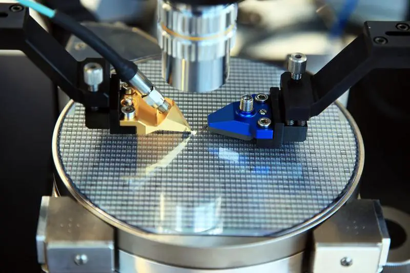
Laser dicing is a highly accurate and precise process that is a perfect match for semiconductor manufacturing. This method is able to handle a wide range of materials and processes, minimizing the risk of cracks, chips, and other defects that can occur when mechanical processing is performed. Further, it can produce thin street widths at high feed rates. The laser-based process can be used to cut a variety of materials, including semiconductors.
A phase-only spatial light modulator can be used to correct the aberration in a semiconductor device. It uses inverse ray tracing to calculate the pattern. The experiment was conducted on 300-um wafers. Compared to the previous procedure, the corrected aberration lengthens multi-depth scan cracks, and increased the dicing speed. Further, the improved ablation correction also improves the quality of the dicing.
Laser dicing is a versatile technology for cutting various kinds of semiconductors. It can be applied to copper, aluminum, and silicon substrates. In addition, the process does not cause any cracks or chips, and is a cost-effective solution for this purpose. This technology also provides the highest level of accuracy for cutting semiconductors. If you're looking for a precision solution, opt for a laser dicing system with a high damage threshold.
Although laser-based dicing processes have many advantages, it is important to choose the right laser-based wafer dicing system for your application. The laser beam must be of high precision and high-velocity in order to achieve the highest dicing yields. With the correct parameters, this technology can produce uniform, quality chips. Its benefits include: a low cost, no tool wear, and no tool dressing.
Laser dicing is a very useful technology for silicon wafers. It offers the benefits of high-feed rate, non-contact dicing, and no chipping. It also eliminates the need for a dressing process and tool wear. With a high feed rate, it can produce very fine kerf facets. However, the advantages of laser-based slicing are still relatively limited.
There are many advantages to laser based dicing for silicon wafers. These include high-feed rates, no chipping, and low tool wear. The laser dicing process also requires no tool wear and no dressing process. The advantages of laser dicing are significant. The accuracy and speed are improved significantly. It is also compatible with other types of silicon wafers. And it is very easy to use.
In addition to the high-throughput and high-resolution of the process, laser-based dicing improves yield. The process is efficient and can be automated. But, there are some disadvantages, such as the poor thermal stability of water-soluble resins. The thermal stability of a laser-based dicing system is also important because it is critical to obtain a high-quality dicing die.
Laser dicing eliminates most debris from a wafer. This results in less backside crack and surface chipping. It also avoids flaking and cracking along the cutting line. A good quality edge is essential for fracture resistance. A high-quality edge means a strong die. If you don't have a good edge, it's unlikely to survive in the package. Hence, a high quality die increases the efficiency of the process.