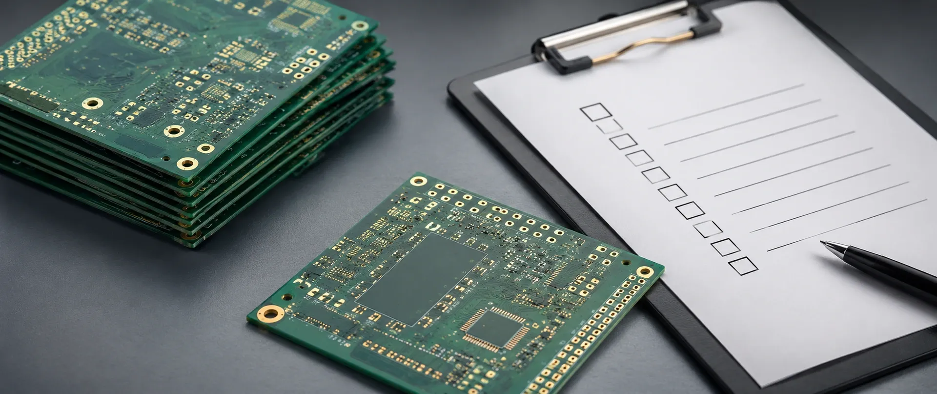

Submitting a PCB design for manufacturing is not simply a matter of exporting Gerber files and placing an order. A complete fabrication package should clearly communicate the electrical, mechanical, and manufacturing requirements of the board. Missing information, outdated files, or conflicting specifications can result in clarification requests, production delays, and unnecessary revisions.
For engineers working on prototypes as well as production boards, using a PCB Fabrication Order Checklist before submission can help ensure that the manufacturing package is complete and consistent.
1. Verify the Gerber Files
Gerber files provide the graphical manufacturing information required to fabricate a PCB. Before sending them to a manufacturer, engineers should confirm that the files were generated from the latest approved PCB design.
Check that all required copper, solder mask, silkscreen, paste, and board outline layers are included. File names and layer descriptions should also be clear enough for the fabrication team to identify their purpose.
It is also useful to review the Gerber package in a viewer before submission. This can reveal missing layers, incorrect artwork, or alignment problems that may not be obvious from the design software alone.
2. Check Drill and Hole Information
Drill data is another essential part of a PCB manufacturing package. NC drill files should accurately represent the hole sizes and locations used in the final design.
Engineers should verify:
- Plated and non-plated holes
- Finished hole sizes
- Slot information
- Drill drawings
- Hole locations
The drill data should correspond with the latest PCB layout. Any mismatch can require additional engineering clarification before fabrication starts.
3. Confirm the PCB Stackup
The stackup defines how the PCB's copper and dielectric layers are arranged. It can influence board thickness, signal integrity, impedance performance, and manufacturing feasibility.
Before submitting an order, confirm the total layer count, dielectric materials, copper thickness, finished board thickness, and any controlled-impedance requirements.
For high-speed designs, providing the intended impedance requirements and relevant stackup information can help the fabrication team determine whether the requested electrical characteristics can be achieved.
4. Review the Board Outline
The mechanical outline should be consistent across the PCB layout, fabrication drawing, and manufacturing files. Engineers should check the overall dimensions as well as internal cutouts, slots, edge features, and other mechanical details.
An incorrect board outline can affect enclosure fit, panelization, assembly, and downstream mechanical integration. A final mechanical review before ordering can help identify these issues early.
5. Specify Copper Weight and Surface Finish
Copper weight should be clearly defined for the relevant PCB layers, particularly when the design has higher current requirements or special thermal considerations.
The selected surface finish should also be documented. Depending on the application, manufacturers may offer options such as ENIG, HASL, lead-free HASL, OSP, immersion tin, or immersion silver.
Clearly specifying the required finish prevents assumptions during the manufacturing process.
6. Review Solder Mask and Silkscreen
Solder mask and silkscreen details are often overlooked during final file preparation. However, incorrect openings or unreadable markings can create problems during fabrication and assembly.
Check solder mask clearances, required openings, mask color, reference designators, polarity indicators, and revision markings. Silkscreen text should remain readable and should not unnecessarily overlap pads or other critical features.
7. Include Complete Fabrication Notes
Fabrication notes provide manufacturing instructions that may not be fully represented by Gerber and drill files.
Depending on the project, these notes may include:
- Material requirements
- Board thickness
- Copper weight
- Surface finish
- IPC requirements
- Dimensional tolerances
- Special processing instructions
Keeping these notes consistent with the rest of the manufacturing package reduces ambiguity and makes the engineering review more efficient.
8. Check DFM Requirements
A Design for Manufacturability review should ideally take place before the order is released. The review can identify potential issues involving trace width, spacing, drill sizes, annular rings, copper clearances, tolerances, and material selection.
DFM checks are especially valuable when a design uses fine features, high layer counts, unusual materials, controlled impedance, blind or buried vias, or other specialized construction requirements.
9. Confirm Revision Control
One of the simplest but most important steps in a PCB Fabrication Order Checklist is confirming that every submitted file belongs to the same approved revision.
Before uploading the manufacturing package, remove outdated files and verify revision numbers, filenames, fabrication drawings, Gerbers, drill files, and stackup documentation.
A consistent revision-controlled package helps prevent manufacturers from working with an older version of the design.
Final Pre-Submission Review
Before placing a PCB fabrication order, engineers should take a final look at the entire manufacturing package rather than checking individual files in isolation. Gerbers, drill files, stackup information, mechanical drawings, fabrication notes, and special requirements should all communicate the same design intent.
A structured PCB Fabrication Order Checklist makes this final review easier and can help reduce avoidable clarification requests and production interruptions. By verifying manufacturing data before submission, engineers can create a smoother transition from completed PCB design to fabrication and support more predictable production workflows.

























Sign in to leave a comment.