

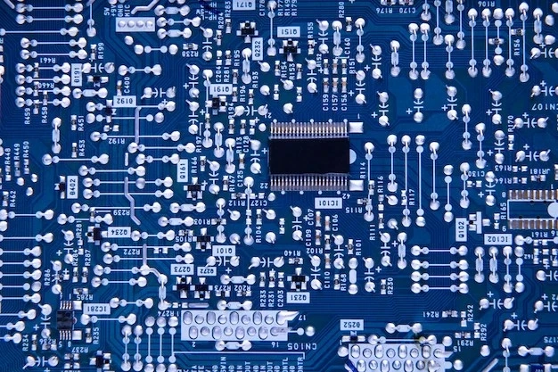
In the PCB industry, it is widely known that copper finishes are applied to the surface of circuit boards. Without proper protection, the copper can undergo oxidation and decay, rendering the PCB useless. The surface finish plays a crucial role as it serves two primary purposes: safeguarding the exposed copper circuitry and providing a solder-able surface for component assembly through soldering. Previously, Hot Air Solder Leveling (HASL) was considered a reliable method for achieving consistent assembly outcomes. However, the constant advancements in circuit complexity and component density have posed significant challenges for horizontal solder leveling systems, pushing them to their maximum capabilities. With the continuous reduction in component pitches and the increasing demand for thinner coatings, the use of Hot Air Solder Leveling (HASL) became a restrictive process for PCB manufacturers. Consequently, alternative coatings, including both electrolytic and immersion processes, have been available as substitutes for HASL for several years. Choose the best PCB manufacturing services in the USA for superior quality and reliable results.
Here are several frequently employed surface finishes in the realm of PCB manufacturing:
HASL / Lead Free HASL
In the PCB manufacturing industry, HASL stands as the prevailing surface finish. This widely adopted process involves submerging circuit boards into a molten tin/lead alloy, followed by the removal of excess solder using ‘air knives’ that blow hot air across the board’s surface. One notable advantage of the HASL process is its inadvertent ability to subject the PCB to temperatures reaching 265°C. This temperature exposure serves as an effective means of detecting any potential delamination issues well in advance, saving valuable resources before expensive components are affixed to the board.
Advantages
AffordableEasily AccessibleRepairableExceptional LongevityDisadvantages
Irregular Surface TextureLimited Suitability for Fine Pitch ComponentsIncludes Lead Content (HASL)Susceptible to Thermal ShockRisk of Solder BridgingPotential Issues with Plugged or Reduced Plated Through Holes (PTHs)Immersion Tin
As per IPC (Association Connecting Electronics Industry) guidelines, Immersion Tin (ISn) is a metallic finish applied through a chemical displacement reaction directly onto the copper base metal of a circuit board. This ISn coating effectively safeguards the underlying copper from oxidation throughout its intended shelf life. However, copper and tin possess a pronounced affinity for each other, leading to an inevitable diffusion process between the two metals. This interaction significantly affects the longevity of the ISn deposit and consequently impacts the overall performance of the finish. The adverse consequences associated with the growth of tin whiskers are extensively discussed in industry literature and form the subject matter of numerous published papers. Experience top-quality PCB manufacturing in the USA. Contact PCB Power Market now to bring your ideas to life!”
Advantages
Smooth Surface TextureLead-FreeRepairablePreferred Option for Press Fit Pin InsertionDisadvantages
Prone to Handling DamageInvolves Carcinogenic Substance (Thiourea)Susceptible to Tin Corrosion on Final AssemblyRisk of Tin Whiskers FormationLimited Suitability for Multiple Reflow/Assembly ProcessesChallenging Thickness MeasurementImmersion Silver
Immersion silver is a chemical finish that does not require electrolysis and is applied by immersing the copper PCB into a silver ion solution. This surface finish is highly suitable for circuit boards requiring EMI shielding, as well as for applications involving dome contacts and wire bonding. The average thickness of the silver coating typically ranges from 5 to 18 microinches. In the context of modern environmental regulations like RoHS and WEE, immersion silver surpasses both HASL and ENIG in terms of environmental friendliness. Moreover, its popularity stems from its lower cost compared to ENIG, making it a cost-effective choice. Looking for reliable PCB manufacturing in the USA? Trust our expertise and precision. Get in touch with PCB Power Market today to discuss your project!”
Advantages
Offers Uniform Application Compared to HASLSuperior Environmental Profile Compared to ENIG and HASLComparable Shelf Life to HASLProvides Cost Advantages over ENIGDisadvantages
Requires Same-Day Soldering On PCB Removal from StorageProne to Tarnishing with Improper HandlingLower Durability Compared to ENIG Due to Absence of Nickel UnderlayerOSP / Entek
OSP (Organic Solderability Preservative), also known as anti-tarnish, safeguards the copper surface from oxidation by employing a conveyorized process to apply an ultra-thin protective layer over the exposed copper. This process utilizes a water-based organic compound that selectively adheres to copper, forming an organometallic layer that shields the copper before soldering. Notably, OSP is exceptionally environmentally friendly when compared to other prevalent lead-free finishes, which tend to be either more toxic or require significantly higher energy consumption.
Advantages
Smooth Surface TextureLead-FreeStraightforward ProcessRepairableCost-EfficientDisadvantages
Difficult to Measure Thickness AccuratelyNot Well-Suited for Plated Through Holes (PTH)Shorter Shelf LifePossible Implications for In-Circuit Testing (ICT)Risk of Copper Exposure in Final AssemblyDemands Careful HandlingOriginal Source: https://primepositionseo.com/2023/06/08/printed-circuit-board-surface-finishes-advantages-and-disadvantages/