
Precision at the Nanoscale: Strategic Imperatives in the Worldwide Photomask Metrology System Market
As semiconductor manufacturing pushes toward the physical limits of lithography, the photomask has evolved from a passive patterning template into a critical precision instrument. The accuracy with which these masks are inspected, measured, and qualified now directly dictates yield, overlay performance, and time-to-volume for advanced logic and memory nodes. Our latest research, the Worldwide Photomask Metrology System Market study, maps this rapidly shifting landscape with the analytical depth required for 2026 corporate planning. The market has demonstrated consistent expansion across the historical review window, with total revenue climbing from approximately 842.15 million USD in 2020 to an estimated 1,280.5 million USD in 2025, and projected to reach roughly 1,352.33 million USD in 2026 before advancing steadily toward 2,211.68 million USD by 2032. This trajectory reflects an anticipated compound annual growth rate of 8.12 percent across the 2025 to 2032 forecast horizon, a pace that signals both sustained capital allocation and an increasingly fragmented strategic environment for equipment buyers, mask producers, and metrology suppliers alike.
The strategic value of this report lies in its ability to convert macro momentum into actionable planning frameworks. Rather than presenting static snapshots, the analysis traces how metrology requirements are being reshaped by high-NA EUV adoption, substrate flatness demands, and tightening export controls on advanced node tools. Buyers entering 2026 must navigate a field where measurement uncertainty, repeatability, and mask-to-wafer correlation are no longer technical footnotes but procurement-critical specifications. The report structures these considerations into a decision-ready format, allowing leadership teams to align equipment roadmaps, capacity investments, and supplier partnerships with the pace of node transitions and mask shop operating models.
Market Architecture and Growth Vectors
Segmentation Dynamics Shaping Procurement Strategy
The market is organized around three primary dimensions that together define where investment pressure concentrates and how vendors differentiate their platforms. By instrumentation type, the landscape spans optical metrology systems, critical dimension scanning electron microscopy tools, and EUV-focused metrology solutions. Optical platforms continue to anchor high-volume registration and overlay verification workflows, while CD-SEM instruments address dimensional repeatability requirements for increasingly complex feature geometries. EUV metrology has emerged as a specialized but strategically vital segment, driven by the need for actinic-capable inspection and registration verification at leading-edge nodes where conventional wavelengths struggle to maintain fidelity.
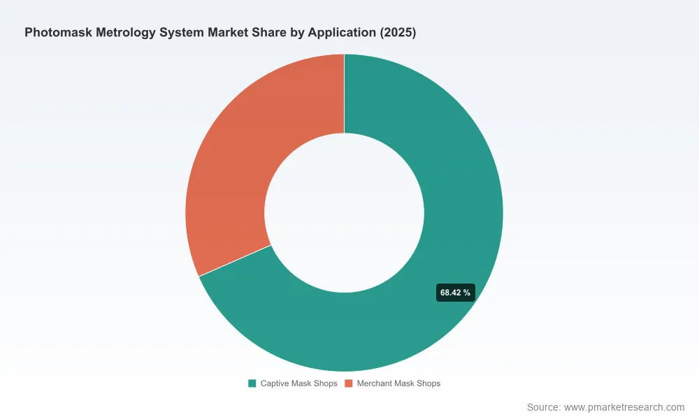
On the application side, demand flows through two distinct operating models. Captive mask shops, typically integrated within large semiconductor or logic manufacturers, prioritize metrology investments that directly support internal volume roadmaps, yield optimization, and proprietary process control. Merchant mask shops, by contrast, operate in a service-intensive environment where throughput, turnaround time, and multi-customer compatibility shape purchasing decisions. Understanding how these operating models diverge in specification priorities, service expectations, and total cost of ownership is essential for forecasting demand patterns and evaluating where vendor lock-in risks or switching opportunities may emerge.
Geographically, the market reflects the concentration of advanced semiconductor manufacturing and mask production capacity across key regions. Asia Pacific accounts for the largest revenue share, reflecting dense concentrations of mask fabrication, foundry activity, and integrated device manufacturer demand. North America and Europe represent substantial and technologically sophisticated markets, each with distinct procurement dynamics shaped by domestic research ecosystems, defense-adjacent semiconductor priorities, and regional equipment supply strategies. The rest of the world contributes a smaller but strategically relevant footprint, often tied to expanding fabrication footprints and localized mask support requirements. The report treats regional distribution not as a static ranking but as a shifting map influenced by fab location decisions, tool qualification cycles, and supply-chain resilience considerations.
Competitive Landscape and Vendor Positioning
Market concentration remains high, with leading vendors commanding a disproportionate share of advanced metrology deployments. This concentration creates both procurement stability and strategic dependency, making competitive intelligence a core input for negotiation strategy and technology roadmapping. The report profiles the companies shaping the market, examining how each positions its metrology portfolio against the evolving demands of sub-nanometer placement accuracy, dimensional repeatability, and flatness characterization.
Carl Zeiss SMT continues to advance registration and overlay metrology platforms designed for sub-nanometer image placement accuracy, with strong emphasis on EUV and advanced node support and robust mask-to-wafer correlation capabilities. KLA Corporation maintains a prominent position through reticle pattern registration metrology systems that support accurate verification of pattern placement across EUV and optical reticles, targeting overlay error reduction in advanced nodes. Mycronic AB provides mask metrology systems oriented toward cost-efficient pattern placement measurement on mature photomasks, leveraging platform synergy to streamline registration evaluation for high-utilization environments.
Worldwide Overlay Metrology System Market
Lasertec Corporation has expanded its focus on advanced EUV mask-related inspection and metrology, including actinic solutions relevant to high-NA EUV photomask qualification for leading-edge manufacturing. Corning Incorporated contributes through flatness metrology instrumentation that supports ultra-low uncertainty measurements of photoblanks and photomasks, an increasingly critical requirement as substrate polishing, coating, and film stress constraints tighten across both DUV and EUV workflows. Advantest Corporation has reinforced its dimensional metrology presence with mask CD-SEM systems aimed at improved reproducibility and curvilinear pattern measurement, aligning with readiness requirements for advanced node geometries. n&k Technology Inc. supports photomask characterization through optical scatterometry-based approaches, including phase shift mask analysis and post-cleaning evaluation, while Vistec Semiconductor Systems supplies critical dimension and pattern placement metrology systems that are deployed across advanced semiconductor device manufacturing environments.
Recent developments illustrate how quickly competitive positioning can shift. In September 2025, Advantest introduced its next-generation Mask CD-SEM system, emphasizing improved CD reproducibility and curvilinear pattern measurement capabilities aligned with 2nm node readiness. In January 2026, Mycronic secured an order for an MMX metrology system for semiconductor photomask pattern placement measurement, underscoring continued demand for registration evaluation platforms in production environments. These events are not isolated product news; they reflect broader competitive dynamics in which vendors race to demonstrate measurement certainty, platform versatility, and alignment with leading-edge lithography requirements.
Forces Reshaping the 2026 Decision Environment
Technical Requirements as Market Drivers
The market is increasingly governed by specification thresholds that directly influence tool selection and qualification timelines. EUV photomask metrology demands sub-nanometer repeatability and accuracy to preserve mask-to-wafer overlay correlation in advanced node production. At the same time, photomask flatness specifications continue to tighten, requiring ultra-low measurement uncertainty systems capable of characterizing quartz substrates and absorber films with greater precision than previous generations of equipment could deliver. As EUV masks grow more complex under high-NA lithography, demand for actinic inspection and registration metrology is intensifying, particularly for high-volume manufacturing of logic and memory chips where defect sensitivity and placement fidelity carry direct financial consequences.
PW Consulting
Supply Chain and Geopolitical Realities
Beyond technical specifications, procurement strategy in 2026 must account for geopolitical and supply-chain pressures. Export controls on advanced semiconductor manufacturing equipment, including metrology tools associated with sub-7nm node support, have introduced friction into global supply chains for photomask production. These controls affect tool availability, qualification pathways, service coverage, and the tempo at which new capabilities can be deployed across regions. For multinational mask operations and integrated manufacturers, this environment elevates the importance of supplier diversification, contingency planning, and region-specific qualification strategies. The report integrates these operational realities into its competitive and regional analysis so that decision-makers can assess not only technological fit but also procurement resilience.
What the Report Delivers
This study is designed as an operational reference rather than a high-level overview. It provides a structured assessment of market sizing, growth pathways, segmentation behavior, and competitive positioning, all interpreted through the lens of procurement and planning relevance. Readers will find detailed coverage of how metrology types interact with mask shop operating models, how regional demand patterns align with manufacturing geography and tool qualification cycles, and how leading vendors differentiate across overlay, CD, flatness, and EUV-specific measurement workflows.
Photomask Market
The report also examines the practical implications of recent product introductions and order activity, translating them into market signal analysis that supports capacity timing, vendor evaluation, and technology investment decisions. Coverage extends to the interplay between measurement uncertainty, process control needs, and total cost of ownership, helping teams compare platforms on more than headline specifications. For organizations evaluating new deployments, expanding mask production capacity, or reassessing metrology supplier relationships, the analysis offers a basis for structured comparison and risk-aware planning.
Why This Research Matters for 2026 Planning
The photomask metrology market is entering a phase in which technical precision, supply-chain fragility, and competitive concentration intersect. Growth is not merely a function of expanding fab output; it is increasingly shaped by node complexity, metrology specificity, and the strategic weight of mask quality in advanced device manufacturing. In that environment, decisions made in 2026 will influence equipment utilization, qualification bottlenecks, and competitive positioning well into the latter half of the decade.
Our Worldwide Photomask Metrology System Market report provides the structured intelligence needed to navigate that environment with confidence. It consolidates market trajectory, segmentation behavior, competitive dynamics, and operational context into a single decision-oriented framework, giving leadership teams the context required to prioritize investments, negotiate from an informed position, and anticipate where measurement demands will intensify next. The full study contains the detailed breakdowns, comparative assessments, and forward-looking analysis necessary to convert market awareness into concrete strategy. For teams responsible for mask production, semiconductor equipment planning, or advanced manufacturing investments, the complete report offers the depth required to act decisively in a market where precision is now a strategic asset.
For detailed analysis of this topic, please visit the official page: Worldwide Photomask Metrology System Market
Lacy Lee
Senior Marketing Manager
[email protected]
PW Consulting: www.pmarketresearch.com

























Sign in to leave a comment.