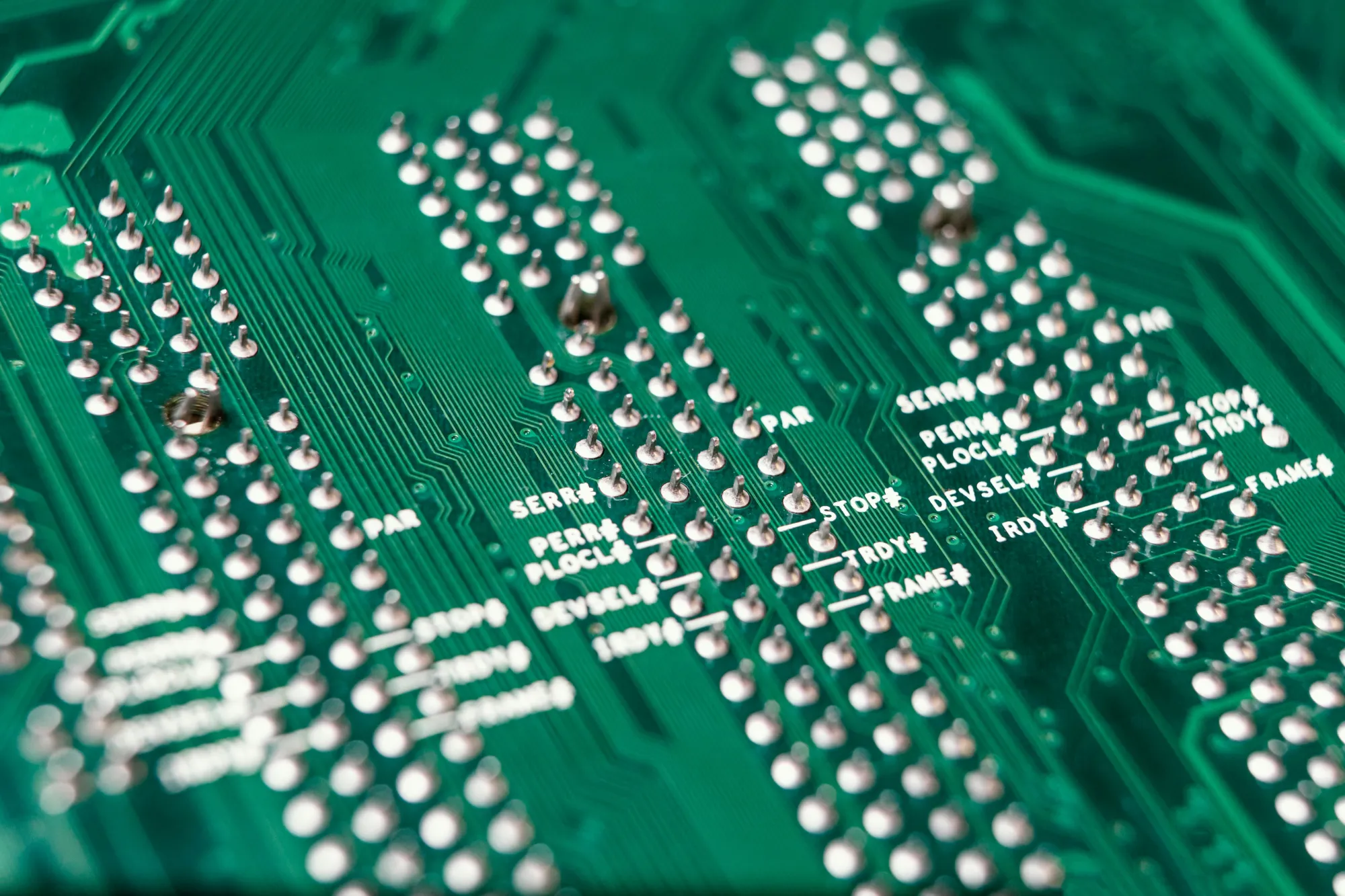

Modern electronic devices are becoming faster, smaller, and more powerful, creating new challenges for PCB designers. Higher data rates, faster switching, compact layouts, and increasing power requirements can introduce signal distortion, noise, electromagnetic interference, and unstable power delivery.
This is why signal and power integrity are essential in high-speed PCB design. Through electrical analysis and simulation, engineers can identify potential problems early and optimize boards for performance, stability, reliability, and manufacturability.
What Is Signal and Power Integrity?
Signal integrity focuses on maintaining the quality of electrical signals as they travel through a PCB. In high-speed designs, impedance mismatches, reflections, crosstalk, and electromagnetic interference can distort signals and affect system performance.
Power integrity focuses on delivering stable and clean power to electronic components. Voltage fluctuations, switching noise, power-plane resonance, and inadequate decoupling can affect sensitive devices.
Although they address different areas, signal and power integrity are closely connected. High-speed signal activity can introduce noise into the power network, while unstable power delivery can affect signal performance.
Why Signal and Power Integrity Matter
As signal transition times become faster, even relatively short PCB traces can behave like transmission lines. Traditional layout approaches may therefore be insufficient for advanced electronic systems.
Poor electrical design can result in:
- Signal reflections and distortion
- Crosstalk between traces
- Electromagnetic interference
- Power supply noise
- Voltage fluctuations
- Timing problems
- Reduced system reliability
Identifying these issues during the design stage can help reduce redesigns, development delays, and hardware failures.
Key Signal Integrity Challenges
Impedance Matching
High-speed signal paths require controlled impedance. Differences between the source, transmission line, and receiver can create reflections that degrade signal quality.
Proper PCB stack-up design, trace dimensions, and controlled-impedance routing help maintain consistent electrical characteristics.
Signal Reflections
When signals encounter impedance discontinuities, part of the signal can reflect toward the source. These reflections may interfere with subsequent transitions and reduce timing margins.
Electrical simulation can help identify discontinuities and optimize high-speed routing before manufacturing.
Crosstalk
When high-speed traces are routed too closely, electromagnetic coupling can create unwanted interference between neighboring signals. Trace spacing, routing direction, reference planes, and stack-up design all influence crosstalk.
Electromagnetic Interference
High-speed transitions and poorly controlled current paths can increase electromagnetic emissions. Proper grounding, return-path management, routing, and shielding can help control unwanted interference.
Power Integrity Challenges
Modern processors, FPGAs, memory devices, and communication components can have rapidly changing power requirements. Maintaining stable power delivery is therefore critical.
Common power integrity concerns include:
- Voltage ripple
- Ground bounce
- Power-plane resonance
- Simultaneous switching noise
- Insufficient decoupling
- Transient voltage variations
- Excessive power delivery impedance
A carefully designed power distribution network helps maintain stable voltage when component current demands change.
Role of Electrical Analysis
Electrical analysis allows engineers to evaluate PCB behavior before manufacturing. Simulation can reveal potential problems without depending entirely on physical prototypes.
Signal integrity analysis can evaluate:
- Transmission-line behavior
- Impedance
- Reflections
- Crosstalk
- Eye diagrams
- Timing margins
- High-speed interfaces
Power integrity analysis can evaluate:
- DC voltage drop
- AC impedance
- Power distribution networks
- Resonance
- Decoupling performance
- Transient response
These insights help engineers make better decisions about PCB layout, routing, stack-up, and power delivery.
Designing PCBs for Better Integrity
Signal and power integrity should be considered from the beginning of the PCB development process.
PCB Stack-Up
The layer structure influences impedance, signal routing, power distribution, and return paths. An appropriate stack-up is essential for high-speed performance.
Return-Path Management
High-speed signals require effective return paths. Reference-plane gaps and discontinuities can increase loop areas and contribute to noise and emissions.
Component Placement
Critical components should be positioned to minimize unnecessary trace lengths and support clean signal and power paths.
Power Distribution
Power planes, vias, decoupling capacitors, and power routes should be designed together to create an effective power delivery network.
Routing Strategy
High-speed interfaces require careful consideration of impedance, trace length, spacing, layer transitions, and length matching.
Benefits of Signal and Power Integrity Analysis
Integrating electrical analysis into PCB development can provide several advantages:
- Earlier issue detection: Engineers can identify electrical problems before prototypes are manufactured.
- Improved stability: Optimized signal and power networks help components operate within required electrical conditions.
- Reduced redesign costs: Simulation can identify problems before expensive board revisions.
- Better high-speed performance: Controlled electrical characteristics support reliable high-speed interfaces.
- Greater design confidence: Analysis provides engineering insight before production.
Building Reliable High-Speed Hardware
As electronic systems become more complex, signal and power integrity must be an integral part of hardware development. Fidus applies electrical analysis, simulation, and PCB engineering practices to address potential challenges before they become costly hardware problems.
The objective is not simply to create a PCB that functions during prototyping. It is to develop hardware capable of delivering consistent electrical performance under real operating conditions.
Conclusion
Signal and power integrity are fundamental to modern high-speed PCB design. From impedance control and crosstalk management to power delivery and return-path design, electrical decisions can directly influence system performance.
By combining careful PCB layout with signal integrity and power integrity analysis, engineering teams can identify risks earlier, optimize designs, reduce redesigns, and develop reliable hardware for demanding applications.
























Sign in to leave a comment.