
The global Gallium Nitride (GaN) substrate market is entering a transformative decade, expanding from USD 0.6 billion in 2025 to USD 1.8 billion by 2035, at a CAGR of 11.9%. GaN substrates are rapidly becoming the cornerstone of modern high-performance electronics — offering high efficiency, superior heat resistance, and faster switching capabilities.
From 5G infrastructure and electric vehicles (EVs) to renewable energy systems and aerospace applications, the demand for GaN substrates is accelerating as industries shift toward energy-efficient, high-power solutions.
Market Overview and Growth Drivers
The surge in the GaN substrate market is driven by the rising demand for high-efficiency power and RF devices, crucial for modern communications and mobility ecosystems.
- 5G Infrastructure Boom: Telecom giants are integrating GaN-on-SiC RF components for next-gen base stations, ensuring high-frequency, low-loss performance.
- EV and Renewable Energy Expansion: Companies like Wolfspeed and Sumitomo Electric are scaling GaN-on-Si production for EV inverters and clean power electronics.
- Semiconductor Innovation: The ongoing transition from silicon-based to wide bandgap materials like GaN is reshaping the global semiconductor landscape.
As these innovations take shape, Asia Pacific — led by China, Japan, and South Korea — is emerging as the most attractive region, with large-scale EV manufacturing, 5G rollout, and renewable energy investments.
Technology Advancements & Industry Initiatives
Technological breakthroughs are strengthening the GaN substrate ecosystem:
- Imec’s 300mm GaN Program (2025): Expanding wafer capacity to accelerate power device development.
- Infineon’s 300mm GaN Production Line: A key step toward high-volume, cost-effective GaN wafer manufacturing.
- Sumitomo Electric’s 6-inch GaN Substrates: Enhancing wafer scalability and processing efficiency.
- Incize ND Atomera Collaboration (July 2025): Aiming to optimize GaN-on-Si device performance for high-frequency applications.
These initiatives mark a strategic move toward larger wafer formats, which improve production yields and reduce costs — making GaN technology more commercially viable across industries.
Key Market Segment: GaN-on-Silicon Carbide (GaN-on-SiC)
The GaN-on-SiC segment dominates the market with nearly 57% share in 2025, thanks to its superior thermal conductivity and reliability. This substrate type is widely used in RF amplifiers, power devices, and high-frequency applications, especially in 5G base stations, EV powertrains, and satellite communication systems.
Companies like Qorvo, Wolfspeed, and IQE plc continue to refine GaN-on-SiC processes to support next-generation power electronics with better power density and durability.
To know more about the GaN Substrate Market- Download our Sample Report
Regional Insights: Asia Pacific Leads the Charge
The Asia Pacific region is spearheading GaN substrate adoption due to its strong semiconductor base and government-backed R&D programs.
- Japan continues to pioneer GaN research, with Osaka Metropolitan University and Sumitomo Electric achieving major fabrication milestones.
- China’s semiconductor initiatives and South Korea’s EV ecosystem are further expanding production capacity.
- India is emerging as a new player, driven by Make-in-India initiatives and increased investment in power electronics and renewable sectors.
The region’s robust manufacturing ecosystem and high-volume semiconductor production make it a hub for both innovation and large-scale GaN integration.
Market Dynamics: Drivers, Restraints, and Opportunities
1. Driver — Advanced Power Electronics Adoption: As industries prioritize high efficiency and compact power systems, GaN substrates deliver unmatched performance in automotive, telecom, and data centers. Their ability to handle high voltages and frequencies makes them ideal for the electrified future.
2. Restraint — Manufacturing Complexity: The production of high-quality GaN substrates remains technically demanding, involving long growth cycles and advanced metrology systems. These challenges sustain higher costs and limit scalability for new entrants.
3. Opportunity — Quantum Computing Integration: Emerging quantum computing applications open new possibilities for GaN substrates. They can operate efficiently under cryogenic conditions, making them suitable for quantum processors and communication systems. This marks a new frontier for GaN utilization beyond conventional power and RF domains.
Key Market Trends: Vertical Integration & Consolidation
The GaN substrate industry is undergoing strategic consolidation as major semiconductor players embrace vertical integration to secure their supply chains.
Notable example:
- Coherent Corp’s acquisition of Sciocs Company (2024) — integrating bulk GaN growth capabilities to strengthen end-to-end control over quality and production.
This trend enables companies to reduce dependencies, streamline development, and accelerate innovation — vital advantages in the rapidly evolving semiconductor ecosystem.
Future Outlook: Towards a USD 1.8 Billion Market
The global GaN substrate market is poised to create an additional USD 1.2 billion opportunity by 2035. The next decade will see:
- A shift toward 8-inch and 12-inch wafers to improve scalability.
- Integration of GaN with AI-driven chip design for data centers and computing.
- Expansion of GaN-on-Diamond and freestanding GaN technologies for next-gen RF systems.
- Increasing investment in quantum, defense, and aerospace electronics.
As industries transition to energy-efficient, high-power solutions, GaN substrates will play a defining role in shaping the semiconductor future.
Closing Thoughts: The Foundation of the High-Performance Era
Gallium Nitride substrates represent more than just an advancement in materials science — they symbolize the foundation of future electronics. From 5G connectivity and EV power systems to quantum computing and space technology, GaN is set to redefine efficiency, scalability, and innovation across industries.
The next decade will belong to technologies that combine performance, sustainability, and intelligence — and GaN substrates are leading that revolution.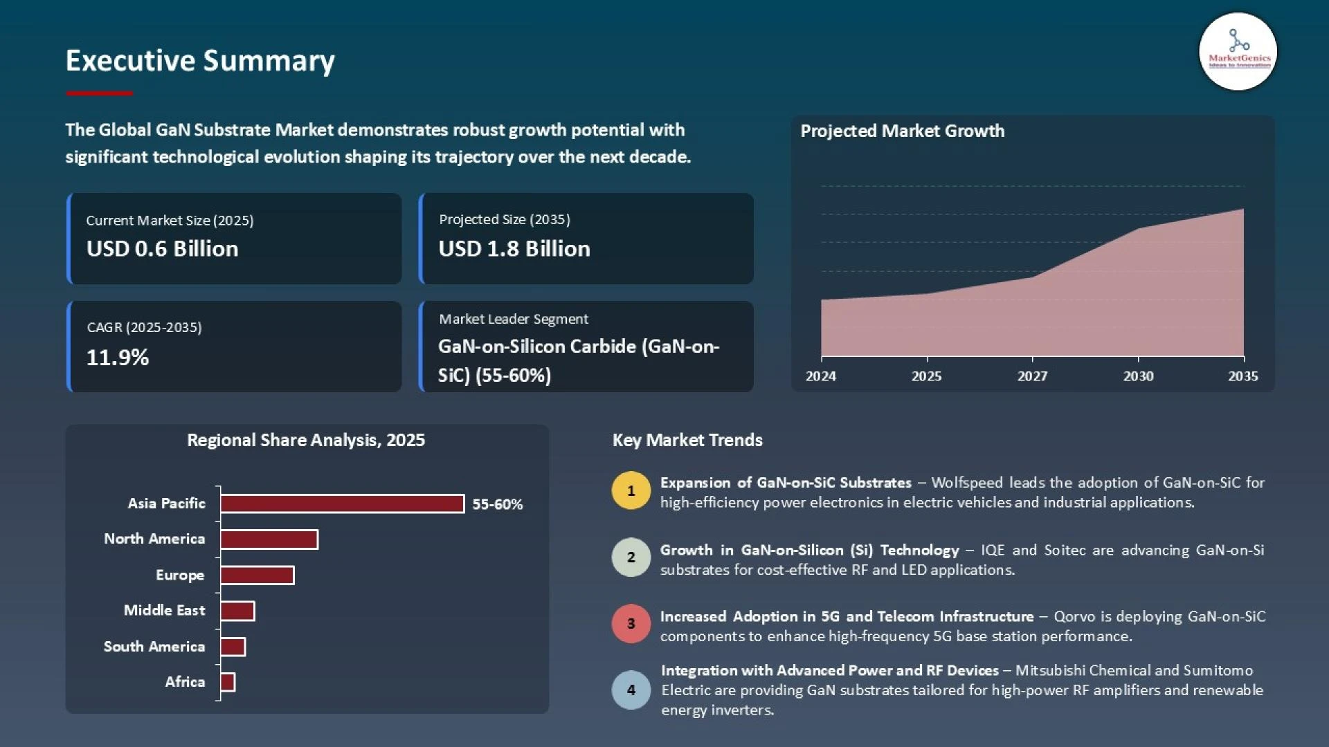


Sign in to leave a comment.