While working on hardware entrepreneurs, many have seen cases of poorly designed PCBs that can never be of adequate quality for commercial production. These boards were designed by freelance engineers or in a few cases, entrepreneurs use to design the PCB. while hiring Prototype PCB Manufacturer, one needs to be careful.
Though it takes an expert professional to review the design of PCB properly, a few ways are also there to judge the design of PCB. In this brief article, we will discuss the ways one can judge the quality of PCB.
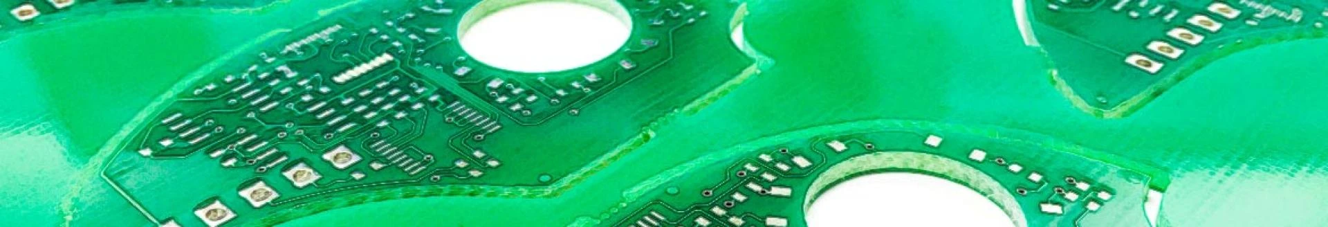
PCB Traces
One needs to look at the visible traces. These traces shall be covered by the solder mask. Solder mask is a thin lacquer kind of layer of polymer and it covers the traces to restrict shorts and oxidation. This layer usually comes in green, different shades are available.
Only to top and the bottom layers are visible and if the PCB board has more than one layer the internal layers shall not be seen. Next, it has to be seen if the traces are running in a straight line with no bends as sharp angles might create trouble for high frequency and high power traces.
Decoupling Capacitors
Every chip needs power for functioning, but what would happen if the power source is far from the chip which needs power? When such a case occurs, power can be brought to the chip through a PCB trace. Decoupling capacitors are very closely placed to the chip's power pins so that any high-frequency noise can be filtered out so that it doesn’t have a negative impact on the chip.
If the chip is having more than one power pin, then each pin needs at least one decoupling capacitor or more. The decoupling capacitors need to be placed very close to the pins. One should know that if in a PCB design the decoupling capacitors are not placed just next to the pin, it's a big indication that the PCB is not designed properly.
Antenna
If the design includes radio revclever or transmitter, then an antenna is mandatory. To get the best performance, the Prototype PCB feedline of the radio frequency pin should be matched to the feedline it is connected to. This feedline has to match the impedance of the antenna.
To maximize the power transfer, impedance matching is necessary. If it's a PCB antenna, the antenna should be at the right edge of the PCB, clear and free of any ground plane. It has to be clear of any traces and also away from large components.
Whether you have outsourced the PCB design to an engineer or you are learning to make a PCB design, judging the quality of PCB design is important. There are many other ways to judge a PCB design.
0


Sign in to leave a comment.