Overview
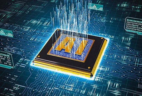
In electronics, AI (artificial intelligence) chips are dedicated processors used to run AI algorithms. The difference from normal chips (CPU/GPU for general purpose) lies in the emphasis on specificity and versatility. CPU, GPU, FPGA, and ASIC chips can all execute AI algorithms. And to a certain extent, GPU and FPGA can also be regarded as AI chips, but ASIC has more distinctive features, so it is also the most representative. So what they are and why they matter?
What is AI Chip?
The so-called AI chips generally refer to ASIC (application-specific integrated circuit) chips. Both traditional CPUs and GPUs can be used to execute AI algorithms, but their speed is slow and performance is not good enough, making them impractical for commercial use. For example, automatic driving needs to recognize road pedestrians, traffic lights and other conditions, but if the current CPU is to calculate, then the car may overturn into the river before calculation results, which is a slow performance. If you use a GPU, the speed is indeed much faster, but the power consumption is high, and the battery of the car may not be able to support normal use for a long time, and the GPU is not economical, that is, ordinary consumers cannot afford it. What’s more, GPUs often out of stock. In addition, the GPU is not an ASIC specially developed for AI, so the speed has not reached its limit, and there is still room for improvement. In fields like intelligent driving requires fast calculation; in mobile terminals, AI applications such as face recognition and voice recognition must have low power consumption. Obviously, GPUs cannot meet the requirements, so the development of ASIC has become inevitable.
Why It Matters?
So why do we need AI chips? For AI algorithms, CNN (convolutional neural network) is commonly used in image recognition and other fields; RNN (recurrent neural network) is mainly used in speech recognition, natural language processing and other fields, which are two different types of algorithms. However, they are essentially matrix or vector multiplication and addition, and then cooperate with division, exponent algorithms.
A mature AI algorithm, such as YOLO-V3, is a large number of calculations such as convolution, residual network, and full connection, which are essentially multiplication and addition. More over, if the specific input graphic size is determined, then the total number of multiplication and addition calculations is determined, like one trillion times, of course, the real situation is much larger than this. If you want to execute it quickly, one trillion additions and multiplications must be performed.
Let’s take another example, such as IBM’s POWER8, one of the most advanced superscalar CPUs for servers, 4GHz, SIMD, 128-bit, assuming that 16bits data is processed, that is 8 numbers, and a maximum of 8 multiplication and addition calculations can be performed in one cycle, performing up to 16 operations at a time. But this is theoretical, it is unlikely in fact.
At this time, the peak calculation times of the CPU in one second = 16X4Gops = 64Gops. In this way, one CPU calculation time can be calculated. And the execution time can also be known by switching to GPU calculation. Let’s talk about AI chips, such as Google’s TPU v1, which is about 700MHz and has a pulsation array of 256X256, as shown in the figure below. A total of 64K units, and each unit can perform one multiplication and one addition at a time, that is 128K operations.
Figure 1: Systolic Data Flow of the Matrix Multiply Unit
In addition to the systolic array, there are other modules, such as activation, etc., which also include multiplication, addition, etc. Look at the peak calculation times of TPU v1 in one second is at least = 128K X 700MHz = 89600Gops ≈ 90Tops, compared with the CPU, you will find that there is a gap of several orders of magnitude in computing capability. Of course, the above data are completely ideal values, and the actual situation may be only 5%. Because the storage on the chip is not large enough, the data will be stored in DRAM, and the data extraction is very slow, then the multiplication logic often has to wait. In addition, the AI algorithm consists of many layers of networks, which must be calculated layer by layer. However, when switching layers, the multiplication logic is free. Therefore, many factors have caused the actual chip to fail to reach the calculation peak.
Although it can be used with slow calculating speed. But at present, the size of the neural network is getting bigger and bigger, and there are more and more parameters. When encountering a large NN model, it takes a few weeks or even a month or two to train, which wastes too much time. If you encounter a sudden situations, such as power outages, have to start all over again. Moreover, if the model is modified, it will take several weeks to know whether it is right or wrong, and no one has so much patience to wait. But with TPU, then you find that you can continue to run by optimizing the parameters during a meal. That is, fast calculation speed enables rapid iteration and development of a stronger AI model.
A deeper comparison can be made clearly for the kernel structure of the GPU. To be sure, the GPU is still relatively fast, at least much faster than the CPU, so most of them currently use the GPU, but don’t forget the GPU disadvantages mentioned earlier, so it is not suitable for large-scale use in data centers. Generally speaking, CPU and GPU are not AI-specific chips. Because they have to realize other functions with other logics inside, which are completely useless for the current AI algorithm. Their performance cannot be used optimally. So it can be seen that it is reasonable for Google to spend money to develop its own AI chip TPU.
AI Chips Design Principles
AI chips follow a hardware design rule: Sacrifice certain versatility to improve the efficiency of specific services. A well-understood example is Bitcoin mining. Bitcoin's basic algorithm is the SHA256, which is based on the hash algorithm, so there is no reverse formula, and it can only rely on mining machines to exhaustively enumerate a large number of possible values. For each block, the miner who first tries to get the correct value will be rewarded. So the faster the calculation, the higher the expectation of winning the reward.
For mining chips, both CPU and GPU have become the mainstream ever. However, as time goes by, GPU mining has become less useful. For example, the RTX3090 graphics card can perform 126.5M SHA256 calculations per second under overclocking conditions, and the total computing power of the entire Bitcoin network has exceeded 178.6EH/s, which is equivalent to the sum of the computing power of 1.4 trillion RTX3090 chips. Therefore, the current mainstream is ASIC mining, which are designed for the SHA256 algorithm, so ASIC mining far better than GPU, and even a single mining machine can overcome supercomputing centers. However, ASIC mining sacrifice generality in hardware, making it impossible to perform other computing tasks, and even unable to mine non-SHA256 algorithm blockchain currencies, such as Ethereum (which is a technology that's home to digital money, global payments, and applications. ).
In the example of Bitcoin mining, it can be seen that a dedicated chip is the most suitable: the algorithm or operator is fixed, and it is relatively simple in the application scenario. The AI chip has the same characteristics as the mining machine, emphasizing the computing efficiency in special scenarios, but the implementation scenarios are different.The purpose of the AI chip is to execute AI algorithms efficiently, so it is also called an AI accelerator. In addition, a bunch of other names are derived, such as NPU (neural network processor), TPU (Google’s tensor processor), APU ( AMD’s accelerated processor), whose properties are very similar.
AI Chip Classifications
AI chips can be divided into two categories. One is for both training and inference, and GPU or CPU can also do it, FPGA (Altera's Stratix series) either, but the TPU v2 and Bitmain's sophon may have an advantage in energy consumption. Compared with GPU, it retains a considerable number of floating-point processing units (or building a lot of tensor computing units), discards some useless graphics pipelines, and improves the energy consumption. There are fewer players in this part, but they are more interesting. For example, ICLR is also thinking about training with fixed-point devices, while Xilinx hopes that XNOR-net can allow fixed-point devices to participate in training.
The other type is the inference accelerator chip, which simply means running the trained model on the chip. This piece is really full of flowers, such as the Cambrian NPU, Intel Movidius (there is also a Nervana that should be similar to XeonPhi for training), Shenjian DPU, Horizon BPU, Imagination's PowerVR 2NX, ARM's Project Trillium, etc. This type of product provides IP for all developers to integrate deep learning accelerators into SoCs.
In addition, we need to talk about Tegra X2 separately. This is equivalent to a small desktop platform. The ARM processor plus Nvidia GPU can provide complete training and inference capabilities. Of course, the power consumption is also high. For other acceleration chips, I think it is best to divide them into two categories, floating-point and fixed-point. Floating point is only FP16 half-precision, of course, it supports FP16 and INT8, such as Cambrian’s NPU and Intel ‘s Movidius. In terms of fixed-point, it is easy to think of Horizon BPU and Imagination's PowerVR 2NX.
Development of AI Chips
Here we will take Google TPU as an example.
1. Parallelization
In order to better accelerate the reasoning of the model, it is necessary to summarize the characteristics of the actual model, find problems, and then make targeted optimization. The algorithm of the AI chip is usually based on the convolutional neural network. Faced with its huge amount of calculation, the CPU can only perform limited calculations in a single clock cycle, and calculation bottlenecks are prone to occur. Where the GPU improves the performance of parallel computing, and converts the equivalent transformation of the convolution operation into a multiplication and addition operation of the matrix, which has become the mainstream hardware for neural network training.
The core of model acceleration is to increase the level of parallelization and perform as many operations as possible in the same clock cycle. So the TPU redesigns a dedicated hardware architecture: the systolic array.
See the figure below for the systolic array of the TPU. The calculation results are not directly output, but "flow" in the array according to the law, and saved after the calculation is completed. It not only increases the degree of parallelism, but also realizes the reuse of parameters and avoids repeated loading. And this array can perform 65536 multiplication and addition operations of 8-bit integers per clock cycle. Under the main frequency of 700MHz, an amazing computing power of 65536 * 700,000,000 * 2 =92Tops@INT8 is realized.
Figure 2: TPU-Systolic-Array
2. High-speed On-chip Storage
Google mentioned that in the neural network it deploys, the number of parameters ranges from 5 million to 100 million, and the intermediate results also have a large amount of data. If the convolution operation unit (such as a systolic array) is frequently performed from DDR:
1) Load parameters
2) Read data
3) Write results
Similar to the barrel effect, it is the shortest piece of wood that determines the water capacity, which is the performance bottleneck. The above-mentioned intensive DDR read and write operations make the IO speed easy to become the performance bottleneck of model reasoning. Therefore, TPUv1 is equipped with 28M bytes of on-chip memory (OCM). Although the cost is relatively high, the read and write speed is far superior to that of DDR. What’s more, the TPUv2 is equipped with 16GB of HBM storage, and its IO speed reached 600GB per second.
With a cache (OCM or HBM), frequently used parameters can be loaded into the cache in advance at runtime, and then the convolution kernel can quickly read the data without repeatedly loading from memory. Not only that, the on-chip memory can also save the intermediate results of the network operation, avoiding transfer (write + read back) on the memory, thereby significantly reducing the IO pressure of the memory.
The role of the cache here is similar to the L3 in the traditional CPU. The purpose is to effectively lower the pressure on the memory, so that the powerful computing power of the convolution kernel can be fully utilized, to avoid the situation of invalid waiting for data loading.
And the paper 2 experiments and counts the running performance of several mainstream models on TPU/GPU/CPU.
The horizontal axis is the required computing power divided by the amount of data that needs to be counted from the memory, which represents the computing density corresponding to the unit memory data loading, while the vertical axis is the actual computing power. Therefore, the slash part represents that the computing performance is restricted by the memory IO bandwidth, while the horizontal part represents that the performance has been fully utilized.
Figure 3: Operational Intensity: Ops/weight byte (log scale)
As shown in the figure, TPU is significantly better than CPU and GPU at high computing density. It can be seen that under high computing density, TPU can play a greater advantage.
3. CNN Quantization Algorithm
In addition to hardware design, in order to make the AI chip run the model more efficiently, it is necessary to perform lightweight processing on the AI algorithm, which can significantly reduce the size of parameters and the amount of calculation. The current neural network training is basically based on floating-point operations. When training and reasoning on the GPU, 32-bit or 64-bit is usually used to represent a floating-point number. If a lower number of bits is used, such as using 8 bits to represent numbers, the parameter size and calculation amount will be greatly reduced.
The figure below uses an 8-bit integer Q to approximate a 32-bit floating-point number.
Figure 4: 32 bit float
This operation brings a certain quantization noise, and a good neural network will have a certain anti-noise ability, so the accuracy loss of the algorithm after quantization will be limited and controllable. Another advantage of quantization is that if the input and parameters of the model are quantized into integer numbers (such as int8/uint8), there is no floating-point calculation, which can simplify the hardware design. As mentioned above, the first-generation TPU only supports integer operations, not only because integer operations are more efficient in hardware, but also because the circuit is much simpler.
At present, there are two mainstream quantification methods:
QAT uses the quantization operator when training the model. It can avoid the loss of precision to the greatest extent, but it cannot use the existing floating-point model and needs to retrain the model from scratch.
PTQ is to quantify the existing floating-point model, although the accuracy and efficiency of the model are not as good as QAT, there is still a great demand for use because there is no need to retrain the model and the threshold for use is lower. Here is a point, how to reduce the loss of accuracy is the goal of the PTQ program, and it has also produced a variety of ideas, such as linear quantization and logarithmic quantization.
4. Efficiency and Cost
In addition to the essential 3x3 convolution, there are dozens of common neural network operators. Because of the chip cost, design difficulty, and operating efficiency, existing AI chips can only support some operators. Therefore, it is necessary to understand and consider hardware capabilities during model training, and try to use operators that can be efficiently supported by AI chips to improve efficiency after deployment. Conversely, when designing the hardware of the AI chip, it is also necessary to consider the needs of algorithm design, and try to support more commonly used operators to improve the degree of freedom in model design.
If the manufacturer has the collaborative development capability between hardware, it can achieve a very good balance between model accuracy, chip cost, and inference speed. This is why more and more terminal manufacturers choose self-developed chips, and AI chip manufacturers often package algorithms for sale.


Sign in to leave a comment.