In today’s technology-driven world, electronic systems must deliver high performance, reliability, and efficiency—all within increasingly compact designs. Achieving this balance requires seamless collaboration across three critical areas: hardware design, PCB layout, and IC packaging. When these elements are thoughtfully integrated, they form the foundation for robust, high-speed, and thermally stable electronic products that perform consistently in demanding environments.
The Foundation: Hardware Design
Every successful electronic system begins with a strong hardware design. This stage involves defining the system architecture, selecting appropriate components, and ensuring signal integrity across the design. Engineers focus on creating a hardware blueprint that can handle electrical and thermal stresses while meeting the system’s speed and power requirements.
Proper component selection—such as processors, FPGAs, and power management ICs—sets the tone for the entire design process. A well-structured schematic not only simplifies the PCB layout phase but also ensures the design can scale and adapt as performance demands evolve.
The Bridge: PCB Layout and Signal Integrity
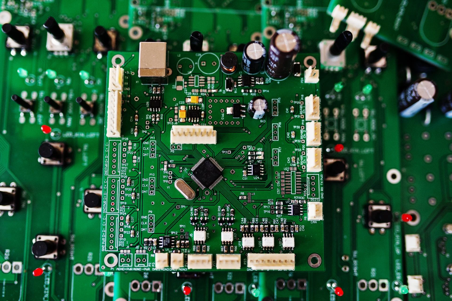
The PCB layout is where the theoretical design comes to life. It determines how electrical signals travel, how components communicate, and how efficiently power is distributed. A carefully planned PCB layout minimizes noise, crosstalk, and electromagnetic interference—key factors in ensuring signal integrity and performance.
Designers must consider trace width, layer stack-up, grounding strategies, and differential pair routing to optimize high-speed communication. Thermal management also plays a vital role; components generating heat must be placed strategically to maintain system stability. Even minor layout decisions, like via placement or decoupling capacitor positioning, can have a significant impact on the overall reliability of the system.
The Core: IC Packaging and Miniaturization
While PCB layout focuses on the board level, IC packaging zooms in on the chip itself. Packaging influences not only how the chip connects to the PCB but also how effectively it manages heat and transmits signals. As devices become smaller and faster, advanced packaging technologies—such as flip-chip, wafer-level, and system-in-package (SiP)—enable higher density, better electrical performance, and improved heat dissipation.
The right packaging choice ensures compatibility between the chip and board, reducing parasitic effects and enhancing power efficiency. In high-speed or high-frequency applications, these design considerations become critical to maintaining stable performance.
Key Benefits of Integrated Design
When hardware design, PCB layout, and IC packaging work together, the results are measurable and impactful. Some of the major benefits include:
- Enhanced System Reliability: Reduced chances of component failure or signal degradation.
- Improved Thermal Performance: Better heat dissipation across chips and boards.
- Optimized Power Efficiency: Lower power losses and improved battery life in portable devices.
- Faster Time-to-Market: Reduced redesign cycles through early collaboration and simulation.
- Scalability: Designs that easily adapt to future performance or size requirements.
The Power of Integration
True reliability and performance arise when hardware design, PCB layout, and IC packaging are developed in unison. Collaboration among engineers in these disciplines prevents design bottlenecks, reduces rework, and ensures every subsystem is optimized for the final product’s goals.
For instance, a hardware designer might adjust the schematic based on PCB constraints, or a packaging engineer might suggest changes to improve signal paths. This iterative, cross-functional approach enables the creation of systems that are not only functional but also scalable and manufacturable.
At Fidus, this integrated approach is a core principle, driving innovative and reliable electronic design solutions that meet the evolving demands of modern technology.
Final Thought
In the fast-evolving electronics industry, performance is not achieved through isolated efforts—it’s the result of an integrated design philosophy. By combining the strengths of hardware design, PCB layout, and IC packaging, engineers can build systems that are not only reliable but also ready for the future. As technology continues to advance, the synergy between these three disciplines will remain the driving force behind the next generation of high-performance electronic solutions.
FAQs
Q1. Why is PCB layout critical to electronic system performance?
A well-designed PCB layout ensures proper signal flow, minimizes interference, and improves power distribution, directly impacting the system’s performance and reliability.
Q2. How does IC packaging affect heat dissipation?
IC packaging materials and structures determine how efficiently heat is transferred away from the chip, helping maintain optimal performance and prevent damage from overheating.
Q3. What are some common challenges in hardware and PCB co-design?
Design synchronization, component placement constraints, and managing signal integrity across multiple layers are some of the biggest challenges engineers face.


Sign in to leave a comment.