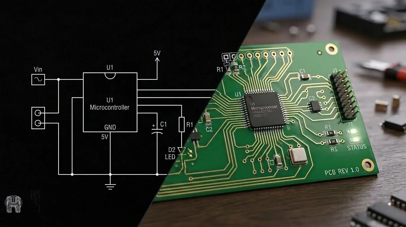

Every electronic product starts with an idea and every idea becomes real through a circuit schematic. But a schematic alone won't get a product manufactured. To go from concept to a physical board, you need to convert that schematic into a PCB layout: the blueprint that defines exactly how components are placed and connected on a real printed circuit board.
Whether you're a student, hobbyist, or professional engineer, understanding the PCB design process is essential. Here's a clear, step-by-step breakdown and how AI PCB design tools like Helektron are changing the game.
What Is a Circuit Schematic?
A circuit is the logical foundation of any electronic device the components and connections that make it function. A schematic is the visual representation of that circuit, showing components like resistors, capacitors, ICs, and even a circuit breaker, connected through labeled signal paths called nets. It defines what connects to what, but not where those connections physically sit on a board.
What Is a PCB Layout?
A PCB (Printed Circuit Board) layout takes your schematic's logic and translates it into physical space. This is where you decide component placement, trace routing, layer stackup, and clearances all while keeping manufacturability and signal integrity in mind. Getting this step right directly impacts performance, cost, and how smoothly your board moves into PCB assembly.
What Is the Difference Between a Circuit Schematic and PCB Layout?
A schematic is a visual representation of an electronic circuit. It uses symbols to show components such as resistors, capacitors, integrated circuits, and connectors, along with the electrical connections between them. A PCB layout, on the other hand, represents the physical arrangement of those components on a printed circuit board. It includes component placement, copper traces, board dimensions, layers, and routing. Before you convert schematic to PCB, the circuit schematic should be complete and verified. Even a small error in the schematic can create problems later during the PCB assembly or manufacturing stage.
PCB Design Workflow: Step-by-Step Guide
The standard PCB design steps to convert a schematic into a working layout includes 5 steps:
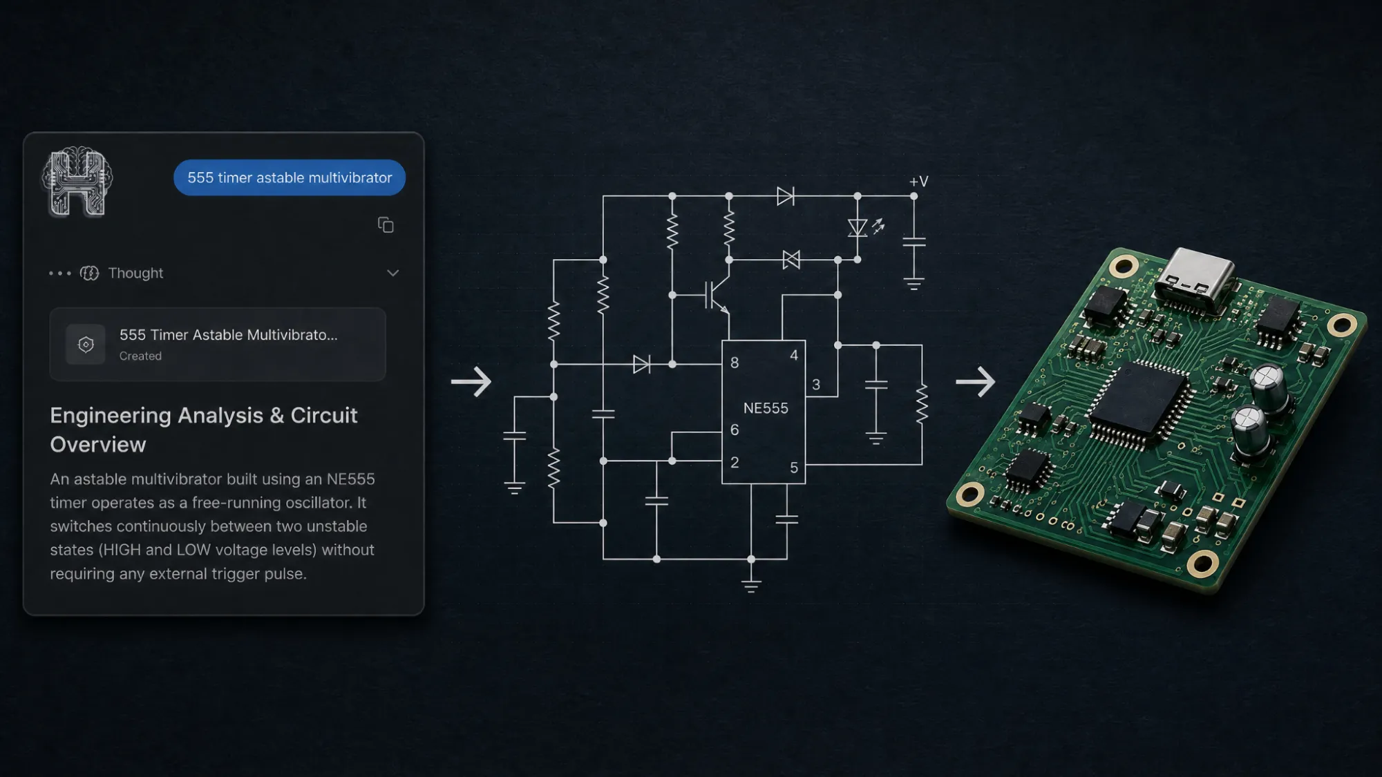
Step 1: Complete and Verify the Circuit Schematic The first step in the PCB design process is creating a complete and accurate schematic. Check that all components have the correct values and footprints and that every required connection is properly defined. Tools such as KiCad and other PCB design platforms allow designers to perform electrical checks before moving to the layout stage. This helps identify missing connections or incorrect component configurations. AI tools are also changing this stage. An AI schematic generator can help transform design ideas into a structured circuit schematic, making the initial stages of AI circuit design more accessible.
Step 2: Assign PCB Footprints to Components To create PCB from schematic, every component must be linked to a physical footprint. A footprint defines the size, shape, and pad arrangement required for mounting the component on the board. For example, two components may have similar electrical functions but completely different package sizes. Selecting the wrong footprint can create major issues during PCB assembly. Always verify footprints using the manufacturer's datasheet before moving forward with the PCB design workflow.
Step 3: Import the Schematic into the PCB Layout Once the schematic and footprints are ready, you can convert circuit diagram to PCB using PCB design software. The software transfers the components and electrical connections into the PCB editor. At this stage, components are typically placed on the board, and connection lines indicate which pins need to be electrically connected. This forms the foundation of the circuit schematic to PCB workflow.
Step 4: Create the PCB Layout Design The next stage is component placement and routing. Place related components close together and consider factors such as signal flow, heat generation, power requirements, and available board space. After placement, copper traces are routed to create the required electrical connections. This is one of the most important PCB design steps, as poor routing can affect circuit performance. Modern AI PCB layout and AI-powered PCB design tools can potentially assist designers by improving workflows, identifying potential issues, and reducing repetitive design tasks.
Step 5: Check and Prepare the PCB for Manufacturing Before manufacturing, run design rule checks to identify spacing, clearance, and connectivity problems. Review the final board carefully before generating manufacturing files. This process is important because errors can increase costs and delay production. Even in applications involving systems such as a circuit breaker, where reliability and electrical requirements are critical, careful design verification is essential.
How Helektron.ai Simplifies the Schematic to PCB Layout Workflow
The traditional process of moving from an idea to a completed PCB can involve multiple tools and complex steps. Helektron.ai helps simplify electronic design by bringing AI-assisted circuit creation and PCB workflows closer together. With features focused on AI PCB design, AI circuit design, and intelligent schematic generation, Helektron.ai can help users move from an initial idea toward a structured circuit and PCB layout design workflow. This makes electronic design more accessible for beginners while supporting a faster workflow for engineers and makers. Understanding how to convert schematic to PCB is an essential skill for anyone involved in electronics. By following a structured PCB design process and using modern tools, you can move more confidently from a circuit idea to a manufacturable board. For further Details contact Team Helektron at +91 87965 06854 Read: AI Schematic Generator: How to Turn a Text Prompt into a Circuit Design Or visit website helektron.ai





















Sign in to leave a comment.