Printed circuit boards (PCBs) are the supporting structure of the electronic devices practically invented in today’s advanced technology. The efficacy and reliability of such PCBs primarily depend on numerous aspects, and the thickness of copper traces is one of the significant parameters. This guide will also cover aspects of PCB FR4 PCB copper thickness regarding the understanding of its relevance, methods of measurement, how to determine an appropriate turn, and much more.
What is a PCB?
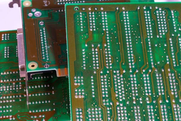
A Printed Circuit Board (PCB) is a critical element in electronics which offers mechanical base and interconnection of many electronic parts. It is a smooth, very hard, non-conductive slab of fiberglass epoxy ; with thin strips of copper foil embedded on one or both surfaces. The copper layers are then photolithographically developed to form the interconnecting paths or ‘traces’ between active components including the resistors, capacitors and integrated circuits ICs and connectors. PCBs form the backbone when it comes to integration of various circuit devices and components, thus offering the solution to efficient assembly method and design of portable gadgets and other complex electrical appliances ranging from television, lap tops, mobile phones right from the boilers, airplanes to pieces of medical equipment and so on.
PCB Board FR4 Copper Thickness
PCBs are made up of laminated structures inclusive of copper layers that act as the pathways or paths that connect the components. FR4 stands for the substrate material, which is a kind of flame retardant fiberglass reinforced epoxy laminate; it is for its durability and electrical insulation. The criterion copper utilized in the fabrication process of PCB in the varied plating thickness directly impacts the board’s electrical performance, reliability, and cost-effectiveness.
Importance of Copper Thickness in PCBs
The thickness of the copper layer on a PCB has significant implications for the board's performance and functionality:
Electrical Conductivity: When the areas of the copper layers are increased, the electrical resistance is lesser, thus allowing good current circulation with minimal power loss.Mechanical Strength: The impact of the copper thickness is evident on the mechanical life of the PCB since it determines the flexibility or rigidity of the board when used in applications such as in bending, vibrations, and other physical interferences.Heat Dissipation: Thicker copper is able to manage the heat better because the higher amount of copper can handle the heat required for high power loads and for devices that are normally at risk of being heat generated.Cost Considerations: Thickness of copper is more costly in manufacturing; nevertheless, when used in large layers, the improvement in cost of the manufacturing aircraft PCBs will be more significant than the enhanced complexity of the circuit.Understanding Copper Thickness Specifications
The metal thickness commonly used is copper thickness measured in ounces per square foot (oz/ft²) or in micrometers (µm) where 1 oz/ft² = 34µm or 1 µm = 0.0000295 oz/ft². 79 µm. Usual copper plating thickness that is used for PCB is 0. Usually, it ranges from 5 ounces per square feet (17.
Variations in Copper Thickness
The choice of copper thickness depends on the specific requirements of the PCB design:
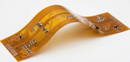
Standard Thicknesses: The majority of PCBs employ copper coatings in a range of 1 to 2 oz per square feet (oz/ft²), because the price increase for thicker copper coatings is not proportional to the added electrical current carrying capacity.Heavy Copper: For high current or graphical mechanical applications, PCBs may use copper weight more than 3 oz/ft² (105 micro-meter) which known as heavy copper PCBs.Flex and Rigid-Flex PCBs: Dependent upon the application flexible and rigid-flex PCBs are inclined to have thinner Copper layers for the nature of flexing and space contour.Manufacturing Considerations FR4 Copper Thickness
Manufacturing processes for PCBs with specific copper thicknesses involve:
Copper Cladding: Adhesion of the copper foil to the substrate, which is most often executed by lamination and/or electroplating techniques.Etching: Copper surface is subjected to chemical etching to achieve the end circuit patterns for the PCB design by stripping off the needed copper materials.Controlled Impedance: The high frequency accuracy enables the ability to control copper thickness furnished for impedance characteristics so vital for signals integrity.Practical Applications and Industry Examples FR4 Copper Thickness
Practical uses of varying copper thicknesses in PCB design include:
Consumer Electronics: It is true that by utilizing thin copper layers, most consumer devices are sufficient, although not the best performing at the most moderate prices.Power Electronics: In addition, one can distinguish high-current arrangements that are supplemented by heavyweight copper printed circuit boards to achieve low voltage drops and high reliability.Telecommunications: RF and microwave PCBs need to have controlled impedance which in turn call for fabrication of specific copper thickness to ensure the integrity of the signal.Challenges and Solutions
Designers and manufacturers face several challenges related to copper thickness:
Cost Optimization: Meeting performance demands while controlling manufacturing costs is a major challenge, with the solutions frequently involving the optimization loops.Heat Management: Thick copper layers help in heat management but it becomes a problem in the manufacturing of the PCB and in assembling.Flex PCBs: Flexible substrates require fewer copper layers because with the bending radii, its thickness should be at its minimum but should not affect its conductivity.Future Trends and Innovations of Copper of FR4 Copper Thickness
Emerging trends in PCB technology related to copper thickness include:
Miniaturization: Finer copper layers contribute to smaller dimensions and allow cutting the costs for the material itself.High-Frequency Applications: Current materials and process development allows for better signal definition through the creation of thinner and highly precise copper layers.Environmental Considerations: The environmentally friendly strategies are used in PCB manufacturing include; minimizing the amounts of materials, which are wasted and energy which is utilized during the entire process.Conclusion
FR4 copper thickness must be comprehended in Prepreg Copper Clustered or PCB board material since it influences the electrical durability, mechanical structure, and cost efficiency of the electronic devices. Thus, making correct decisions over the copper thickness, and applying more advanced technologies in manufacturing allows designers to meet a range of high-performance standards without losing their ability to respond to industry changes . As technology in electronic devices increases, hence does the technologies and procedures on the PCB copper weight increment, subsequently providing optimal, dependable, and eco-friendly solutions to the society in future.


Sign in to leave a comment.