In the field of electronics, the term PCB assembly is a cornerstone concept that plays a crucial role in the functionality of electronic devices. Understanding what PCB assembly is and how it works can offer valuable insights into the manufacturing process of countless electronic products we use daily, from smartphones and laptops to medical devices and automotive systems. This article delves into the intricacies of PCB assembly, exploring its components, processes, benefits, and more.
What is a PCB?
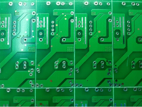
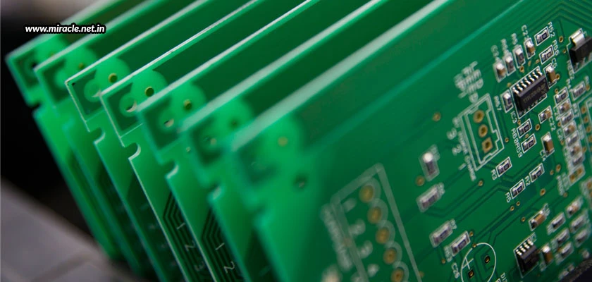
Before diving into PCB assembly, it’s important to grasp the basics of a Printed Circuit Board (PCB). A PCB is a physical platform that provides the electrical connections and mechanical support for electronic components. It consists of a non-conductive base material, typically fiberglass or epoxy resin, with conductive pathways etched or printed onto its surface. These pathways, or traces, connect various electronic components such as resistors, capacitors, and integrated circuits, allowing them to communicate and function as intended.
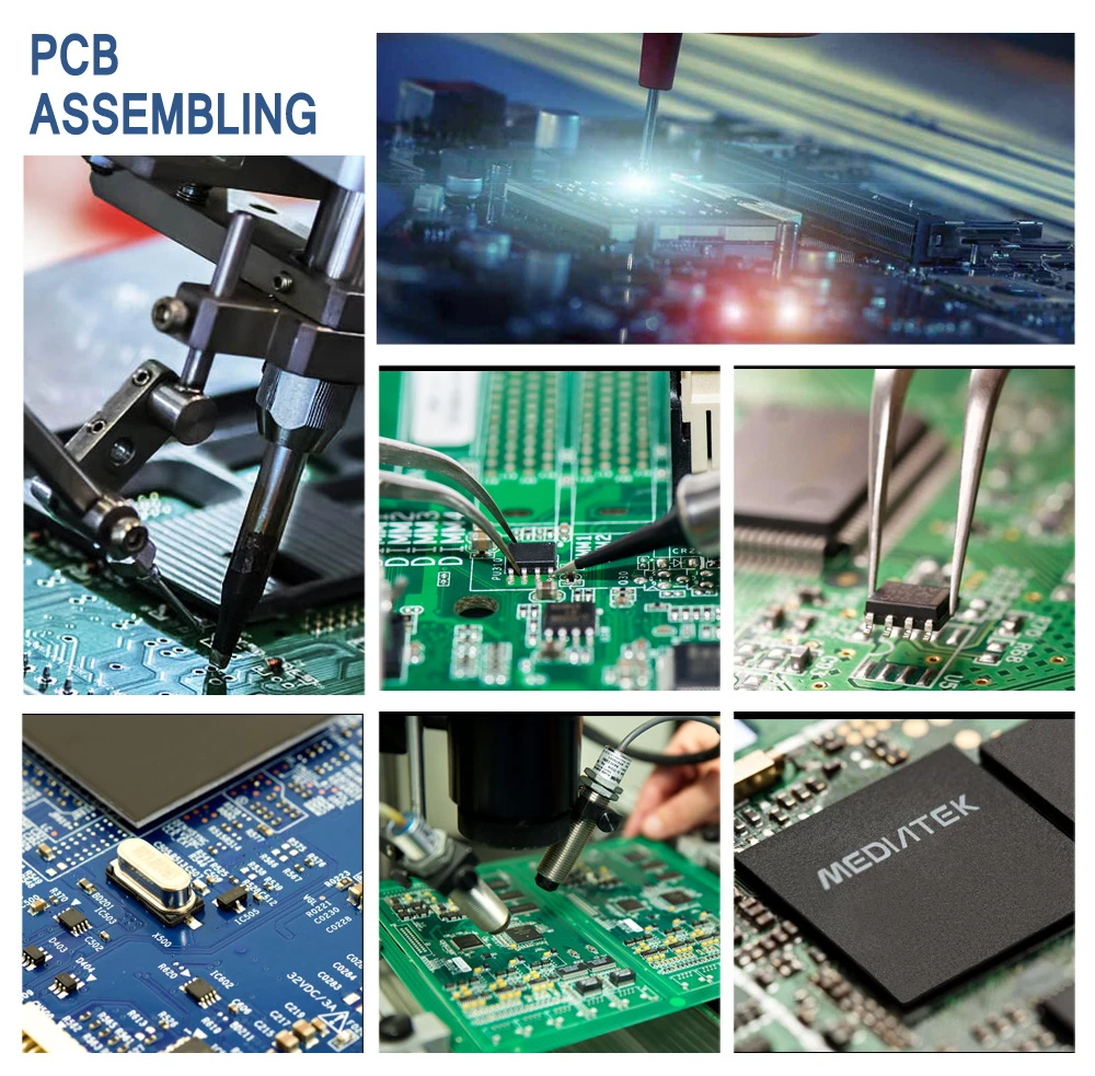
The PCB Assembly Process
PCB assembly refers to the process of mounting and connecting electronic components onto a PCB. This process is integral to creating functional electronic devices. The assembly process can be broken down into several key stages:
1. Design and Prototyping
Before assembly begins, a detailed PCB design must be created. This design involves laying out the circuit schematic, determining component placements, and routing electrical connections. Modern design software helps engineers create precise designs that meet specific electrical and mechanical requirements. Prototyping involves creating a sample PCB to test the design before mass production.
2. Solder Paste Application
The first step in the actual assembly process is applying solder paste to the PCB. Solder paste, a mixture of solder powder and flux, is applied to the pads on the PCB where components will be placed. This is usually done using a stencil and a squeegee to ensure an even and accurate application.
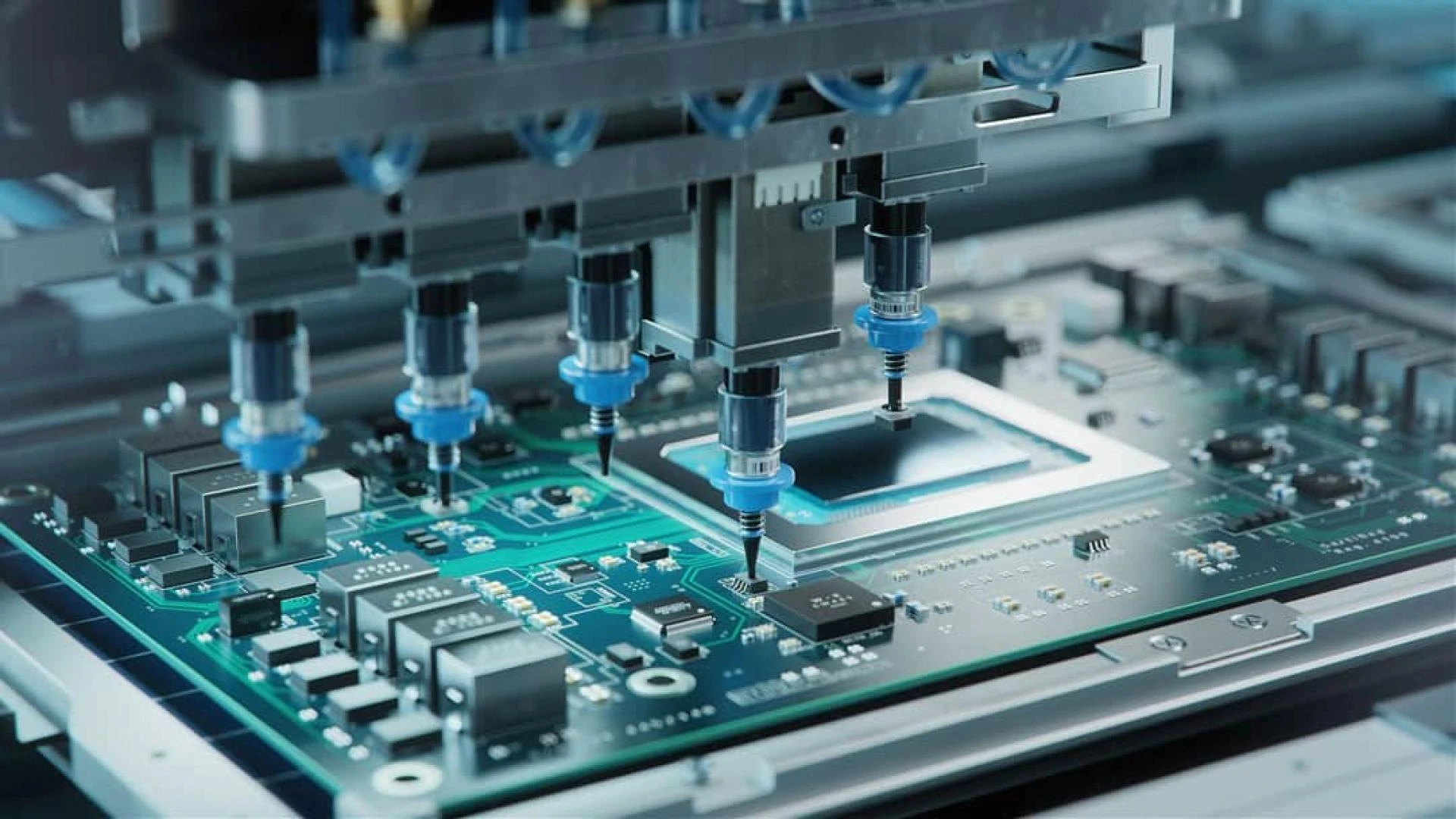
3. Component Placement
Once the solder paste is applied, electronic components are placed onto the PCB. This is typically done using automated pick-and-place machines that position components with high precision. For more complex or smaller quantities, manual placement might be used, though it is less common in high-volume production.
4. Soldering
After components are placed, the next step is soldering. The solder paste, which was previously applied, is melted to create permanent electrical connections between the components and the PCB. This can be achieved through several methods:
- Reflow Soldering: This involves heating the entire PCB in a reflow oven to melt the solder paste.
- Wave Soldering: This technique is often used for through-hole components. The PCB is passed over a wave of molten solder, which solders the components to the board.
- Hand Soldering: For small production runs or repair work, soldering is done manually using a soldering iron.
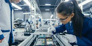
5. Inspection and Testing
Post-soldering, the PCB assembly undergoes rigorous inspection and testing. Automated Optical Inspection (AOI) systems are commonly used to detect defects such as misaligned components or solder bridges. Functional testing follows, where the assembled PCB is tested to ensure it operates correctly within its intended application.
6. Rework and Repair
If defects are found during inspection or testing, rework and repair processes are carried out to correct issues. This might involve replacing defective components, re-soldering joints, or correcting design errors.
7. Final Assembly
Once the PCB assembly passes all tests, it is integrated into its final enclosure or product housing. This step may also involve additional assembly work, such as attaching connectors or cables, depending on the end product.
Benefits of PCB Assembly
PCB assembly offers several benefits that contribute to the efficiency and reliability of electronic products:
1. Increased Reliability
Properly assembled PCBs ensure that electronic components are securely connected, reducing the risk of failures or malfunctions. Reliable PCB assemblies are crucial for high-performance and safety-critical applications.
2. Compact Design
PCB assemblies enable the integration of numerous components into a compact, organized layout. This space-saving aspect is essential for modern electronics, where miniaturization is often a key design goal.
3. Cost Efficiency
Automated PCB assembly processes, especially in high-volume production, can significantly reduce labor costs and production time. Additionally, the precision of automated systems helps minimize material wastage and rework, further contributing to cost efficiency.
4. Consistency and Quality
Automated processes and rigorous quality control measures ensure consistent and high-quality PCB assemblies. This consistency is crucial for maintaining the performance and durability of electronic devices.
Conclusion
PCB assembly is a fundamental process in electronics manufacturing that involves mounting and connecting components on a printed circuit board to create functional electronic devices. From the initial design to the final inspection, each step in the PCB assembly process plays a vital role in ensuring the reliability, efficiency, and performance of electronic products. As technology continues to advance, the techniques and practices surrounding PCB assembly will evolve, further enhancing the capabilities and applications of electronic devices.
FAQs
1. What is the difference between PCB design and PCB assembly?
PCB design refers to the creation of the schematic and layout of a printed circuit board, including the placement of traces and components. PCB assembly, on the other hand, involves the physical process of mounting and soldering components onto the designed PCB to create a functional product.
2. What materials are commonly used for PCBs?
Common materials used for PCBs include fiberglass-reinforced epoxy (FR-4), paper phenolic, and ceramic. FR-4 is the most widely used due to its excellent mechanical and electrical properties.
3. Can PCB assembly be done manually?
Yes, PCB assembly can be done manually, especially for small-scale production or prototyping. However, automated assembly is typically used for larger production runs due to its speed and precision.
4. What are common defects in PCB assembly?
Common defects in PCB assembly include solder bridges, misaligned components, insufficient solder joints, and component placement errors. These issues can be detected and corrected through rigorous inspection and testing processes.
5. How does reflow soldering work?
Reflow soldering involves melting solder paste applied to the PCB using a reflow oven. The oven heats the PCB to a specific temperature, allowing the solder paste to melt and form solid connections between components and the PCB.
Sign in to leave a comment.