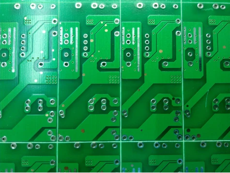
1. What is PCB Delamination?
At its core, PCB delamination refers to the undesirable separation of layers within a printed circuit board. PCBs are constructed from multiple thin layers of conductive copper foil and insulating dielectric substrate (often fiberglass impregnated with resin, known as prepreg), all pressed and bonded together under heat and pressure.
2. Common Causes of PCB Delamination
2.1 Thermal Stress
One of the most significant contributors to delamination is thermal stress, particularly during PCB manufacturing and PCB assembly processes. The rapid heating and cooling cycles that PCBs undergo can put immense strain on the laminated layers.
2.2 Moisture Absorption
Moisture is a silent saboteur of PCBs. The dielectric materials used in PCBs are often hygroscopic, meaning they can absorb moisture from the surrounding environment. If a board with absorbed moisture is subjected to high temperatures (e.g., during soldering), the trapped water rapidly vaporizes into steam. This steam creates internal pressure that can physically push the laminate layers apart, leading to blistering and delamination. Proper storage and pre-baking processes are essential to mitigate this risk.
3.Strategies for Preventing PCB Delamination
Material Selection
- HighTg Laminates: Choose laminate materials with a glass transition temperature (Tg) significantly higher than the maximum temperature the PCB will experience during assembly (e.g., reflow) and operation.
- Matched CTEs:Select materials with similar Coefficients of Thermal Expansion (CTE) to minimize stress build-up during temperature fluctuations.
- Low Moisture Absorption:Opt for materials with low moisture absorption rates, especially for applications in humid environments or those undergoing high-temperature processing.
Optimized Manufacturing Processes
- Controlled Reflow Profiles:Carefully calibrate reflow oven temperature profiles to ensure proper soldering without exposing the board to excessive heat or prolonged dwell times. The reflow profile should be optimized for the specific materials and components used.
- Proper Pre-Baking:Before assembly, PCBs should be pre-baked (or “dry baked”) to remove any absorbed moisture. This is a critical step, especially for boards that have been stored for extended periods or in humid conditions.
- Optimal Lamination Parameters:During PCB fabrication, strict control over lamination pressure, temperature, and curing cycles is necessary to ensure robust interlayer adhesion.
- Careful Handling:Minimize mechanical stress during all stages of manufacturing, from handling raw materials to final assembly.
Design Considerations
PCB micro-section analysis and surface thermal distribution
- Balanced Copper Distribution:Distribute copper evenly across all layers to prevent localized hot spots and uneven thermal expansion.
- Via Design:Ensure proper via plating and aspect ratios to avoid stress concentrations around barrel walls, which can initiate delamination during thermal cycling.
Quality Control and Testing
- Incoming Material Inspection:Verify the quality of raw materials (laminates, prepregs, copper foils) before they enter production.
- In-Process Monitoring:Implement continuous monitoring of temperature, pressure, and time parameters during lamination and assembly.
- Regular Testing:Conduct routine reliability tests such as thermal cycling, humidity testing, and periodic micro-sectioning to validate the manufacturing process and material performance.


Sign in to leave a comment.