Every device that processes, stores, or transmits digital information depends on a component most people never see: the semiconductor silicon wafer. From the smartphone in your pocket to the data center running the cloud service you used this morning, semiconductor silicon wafers are the physical substrate on which modern electronics are built.
What a Semiconductor Silicon Wafer Actually Is
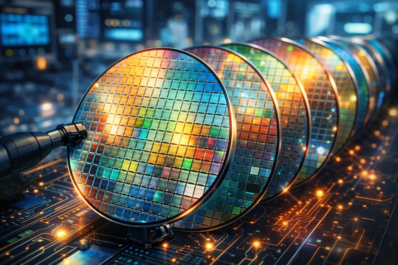
A semiconductor silicon wafer is a thin, flat disc of highly purified crystalline silicon used as the base material for manufacturing integrated circuits and other microelectronic devices. The wafer serves as the physical platform onto which transistors, capacitors, resistors, and interconnects are fabricated in layers through a photolithographic process.
The term semiconductor refers to a material whose electrical conductivity falls between that of a conductor and an insulator. Silicon conductivity can be precisely controlled through doping — the deliberate introduction of small quantities of other elements such as phosphorus or boron.
Why Silicon Dominates Semiconductor Manufacturing
Silicon is the second most abundant element in the Earth's crust. Silicon dioxide formed naturally when silicon is oxidized is an excellent insulator serving critical functions in device fabrication. Silicon has a stable, predictable crystal structure that supports precise atomic-scale fabrication. Silicon bandgap of approximately 1.1 eV makes it well suited to the voltage ranges used in digital logic circuits.
From Sand to Semiconductor Silicon Wafer
Production begins with metallurgical-grade silicon derived from silica. Further purification produces polysilicon with a purity exceeding 99.9999999 percent. From polysilicon, single-crystal silicon is grown using the Czochralski process — a seed crystal introduced into a melt of purified silicon and slowly withdrawn while rotating, producing a large cylindrical single-crystal ingot that can be up to 300mm in diameter.
Wafer Diameter and Its Significance
Semiconductor silicon wafers are produced in standard diameter sizes including 100mm, 150mm, 200mm, and 300mm. Larger diameter wafers provide more surface area per wafer, allowing more chips to be fabricated simultaneously and reducing per-chip production cost.
The Fabrication Process: From Wafer to Chip
A bare semiconductor silicon wafer is the starting point for an integrated circuit fabrication process that may involve hundreds of individual process steps including thermal oxidation, photolithography, etching, doping, deposition, and chemical-mechanical planarization.
Applications Across the Technology Spectrum
The applications of semiconductor silicon wafers extend across processors and memory chips, power semiconductors, MEMS, photovoltaics, and research and development. UniversityWafer supports researchers and engineers working across this full application spectrum with a supply of high-quality silicon and compound semiconductor wafers suited to diverse technical requirements.


Sign in to leave a comment.