

Understanding how to control impedance in RF PCB design can feel a bit like tuning a musical instrument—everything has to be just right for the signal to “play” cleanly. When you’re dealing with high-frequency signals, even small mismatches in impedance can lead to reflections, signal loss, and performance instability. That’s where an RF PCB impedance calculator becomes an essential tool. It helps engineers predict and control how signals behave across traces, layers, and materials before the board is even manufactured.
In modern RF applications like wireless communication, radar systems, and IoT devices, precision is everything. Designers can’t rely on guesswork anymore. They need accurate calculations that factor in dielectric constants, trace width, copper thickness, and spacing between layers. An impedance calculator simplifies this complex process, turning advanced electromagnetic theory into practical design decisions. When used correctly, it saves time, reduces costly redesigns, and ensures the final product performs exactly as expected.
RF PCB Impedance Calculator Guide becomes significantly more effective when supported by the engineering expertise of Shenzhen Rich Full Joy Electronics Co., Ltd, known for delivering precise impedance-controlled PCB solutions tailored for high-frequency applications.
What Is an RF PCB Impedance Calculator?
An RF PCB impedance calculator is a specialized tool that helps designers determine the correct trace dimensions and stackup parameters needed to achieve a target impedance—typically 50 ohms for most RF systems. At its core, the calculator uses mathematical models to simulate how electromagnetic fields interact with PCB materials and geometries. Instead of manually solving complex equations, engineers can input design parameters and instantly get accurate results.
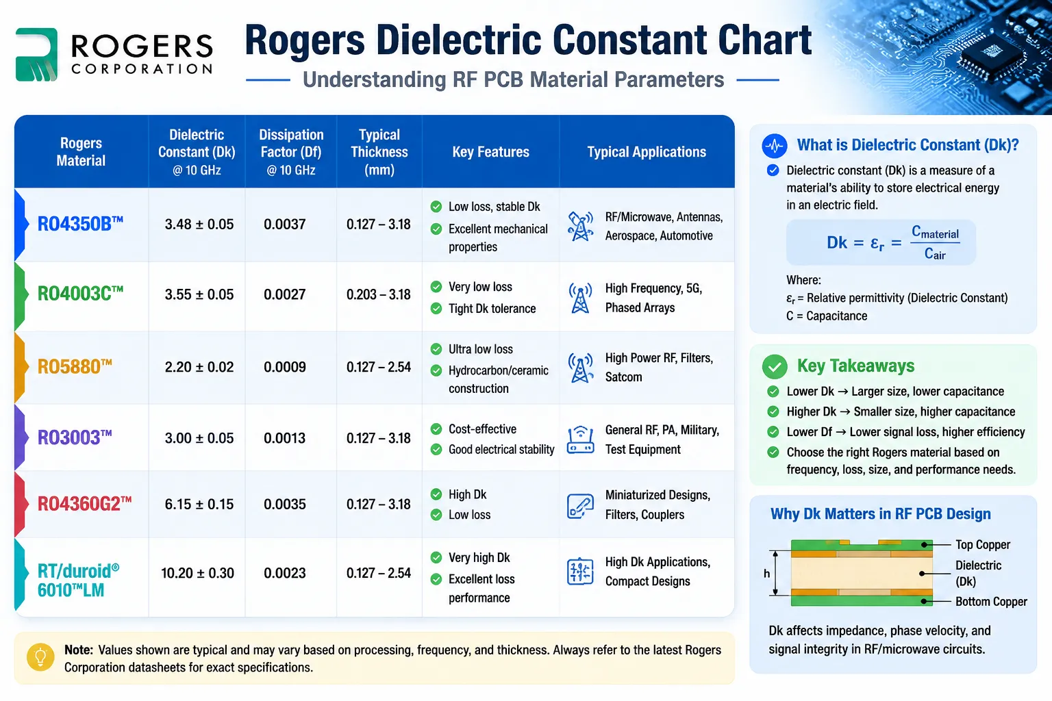
What makes these calculators so valuable is their ability to handle different transmission line configurations. Whether you’re working with microstrip (surface traces) or stripline (internal traces), the calculator adjusts its formulas to match the structure. It considers variables like dielectric constant (Dk), substrate height, copper thickness, and trace spacing. Each of these factors influences how signals propagate, and the calculator brings them all together into a clear output.
Beyond just numbers, impedance calculators also help visualize trade-offs. For example, if you want a narrower trace, the calculator might show that you need a thinner dielectric layer to maintain impedance. This kind of insight allows designers to make informed decisions early in the design process. It’s not just a calculation tool—it’s a design companion that helps balance performance, manufacturability, and cost.
Why Impedance Control Matters in RF Design
Impedance control is the backbone of reliable RF performance. When impedance is properly matched across the entire signal path, signals travel smoothly without reflections or էներգիա loss. But when there’s a mismatch, part of the signal reflects back toward the source, creating interference and reducing efficiency. In high-frequency systems, even a small mismatch can have a noticeable impact.
Think of it like water flowing through a pipe. If the pipe suddenly narrows or widens, the flow becomes turbulent. The same thing happens with electrical signals when impedance changes abruptly. This turbulence shows up as noise, distortion, or reduced signal strength. In RF applications, where signals often carry critical data, this can lead to serious performance issues.
Another important aspect is consistency. It’s not enough to achieve the correct impedance in one section of the board—the entire signal path must maintain it. This includes traces, vias, connectors, and even transitions between layers. An impedance calculator helps ensure this consistency by providing precise design parameters that can be applied throughout the PCB.
Key Inputs Required for Accurate Calculations
Using an RF PCB impedance calculator effectively starts with understanding the inputs. Each parameter plays a role in determining the final impedance, and even small inaccuracies can lead to incorrect results. That’s why it’s important to gather reliable data before running calculations.
Some of the most critical inputs include:
- Dielectric constant (Dk) of the substrate material
- Thickness of the dielectric layer
- Trace width and spacing
- Copper thickness
- Type of transmission line (microstrip or stripline)
The dielectric constant is particularly important because it directly affects how signals propagate through the material. A higher Dk means signals travel slower, which influences impedance. Similarly, the thickness of the dielectric layer determines how far the signal is from the reference plane, affecting capacitance and impedance.
Accuracy is key here. Using generic or अनुमान values can lead to mismatches in the final design. That’s why many engineers rely on verified material data and collaborate with manufacturers like Shenzhen Rich Full Joy Electronics Co., Ltd to ensure their inputs reflect real-world conditions. This level of precision helps bridge the gap between theoretical calculations and actual performance.
Step-by-Step Guide to Using the Calculator
Using an RF PCB impedance calculator might seem intimidating at first, but once you understand the process, it becomes quite straightforward. The goal is to input the right parameters and interpret the results correctly so you can adjust your design accordingly.
Start by selecting the type of transmission line you’re working with—microstrip or stripline. This choice determines which model the calculator will use. Next, enter the known parameters such as dielectric constant, substrate thickness, and copper thickness. These values are usually provided by your material supplier or manufacturer.
Once the base parameters are set, you can either input a desired impedance (like 50 ohms) and let the calculator determine the required trace width, or input a trace width and see what impedance it produces. This flexibility allows you to iterate quickly and find the optimal design.
After getting the results, it’s important to review them in the context of your overall design. For example, a very narrow trace might achieve the desired impedance but could be difficult to manufacture. This is where practical experience and collaboration come into play, ensuring that the design is both functional and feasible.
Microstrip vs Stripline Calculations
One of the key decisions in RF PCB design is whether to use microstrip or stripline configurations, and impedance calculators handle each differently. Microstrip traces are located on the outer layers of the PCB and reference a single ground plane. They are easier to access and test but are more exposed to external interference.
Stripline traces, on the other hand, are buried between two ground planes, providing better shielding and reduced electromagnetic radiation. This makes them ideal for sensitive RF signals. However, they are more complex to manufacture and can be harder to debug.
The impedance calculator accounts for these differences by using distinct formulas for each configuration. For microstrip, it considers الهواء interaction, while for stripline, it focuses on the dielectric environment. Understanding these differences helps you choose the right configuration for your application and use the calculator more effectively.
Common Mistakes to Avoid
Even with a powerful tool like an impedance calculator, mistakes can still happen. One of the most common errors is using incorrect material properties. If the dielectric constant or thickness values are off, the calculated impedance will not match the real-world performance.
Another mistake is ignoring manufacturing tolerances. In practice, there will always be slight variations in layer thickness and trace dimensions. Failing to account for these can lead to impedance mismatches. That’s why it’s important to include tolerance margins in your design.
Designers also sometimes focus too much on calculations and overlook layout considerations. Sharp bends, երկար vias, and inconsistent trace widths can all disrupt impedance, regardless of what the calculator says. A holistic approach that combines accurate calculations with good layout practices is essential for success.
Real-World Applications and Benefits
RF PCB impedance calculators are used across a wide range of industries, from telecommunications to aerospace. In each case, the goal is the same: ensure reliable signal transmission in high-frequency environments. These tools help engineers design boards that meet strict performance requirements without excessive trial and error.
The benefits go beyond just accuracy. By using an impedance calculator, designers can reduce development time, minimize prototyping costs, and improve overall product quality. It allows for faster iterations and more confident decision-making, which is crucial in competitive الأسواق.
Working with experienced manufacturers like Shenzhen Rich Full Joy Electronics Co., Ltd further enhances these benefits. Their expertise ensures that calculated designs are translated into high-quality PCBs that perform as expected in real-world conditions.
Conclusion
Learning how to use an RF PCB impedance calculator is a valuable skill for anyone involved in high-frequency PCB design. By understanding the key inputs, choosing the right configurations, and avoiding common mistakes, you can create designs that deliver consistent and reliable performance. With the right tools and knowledge, impedance control becomes less of a challenge and more of a strategic advantage.
For more expert guidance and advanced PCB solutions, visit https://www.richpcba.com/.





























Sign in to leave a comment.