When designing electronic devices, one of the most important factors to consider is the reliability of the circuit. A crucial part of this is the PCB (Printed Circuit Board) layout, which can greatly impact the performance, durability, and overall lifespan of the product. In this blog, we will discuss some best practices for designing a reliable PCB layout that ensures your hardware works efficiently and lasts longer.
Understanding the Importance of PCB Layout
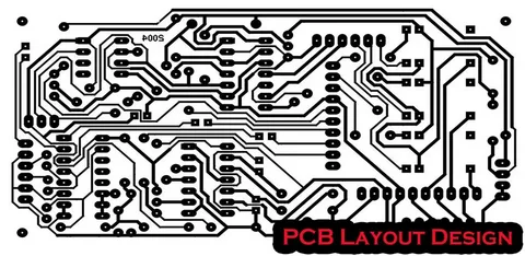
The PCB layout is essentially the blueprint for where all the components of an electronic device will be placed. It defines the paths through which signals and power flow, the connections between different parts, and the overall structure of the circuit. A well-designed PCB layout is vital for reliable hardware performance, while a poorly designed layout can lead to issues such as signal interference, overheating, and even failure of the device.
To achieve a reliable PCB layout, designers need to follow some best practices that help avoid common mistakes and enhance the overall performance of the hardware.
1. Plan Your Component Placement Carefully
One of the first steps in creating a reliable PCB layout is to plan where each component will be placed. This may seem simple, but it requires careful thought to ensure that components do not interfere with each other and are positioned in a way that minimizes issues like signal noise and power loss.
For example, it’s important to separate high-frequency components from sensitive analog circuits. Keep sensitive parts away from noisy areas, such as the power supply, and ensure there’s enough space for heat dissipation around components that generate a lot of heat. Effective placement will also help in reducing the length of the signal traces, making the board more efficient.
2. Maintain Proper Trace Widths and Spacing
When laying out the PCB, the width and spacing of the traces (the conductive paths connecting components) are critical for reliability. If the traces are too narrow, they can become hot and possibly burn out, leading to circuit failure. On the other hand, if the traces are too wide, the PCB becomes unnecessarily large and costly.
Trace width should be determined based on the current that will pass through it. Higher currents require wider traces to prevent overheating. Additionally, ensure proper spacing between traces to avoid short circuits or unintentional connections. Using tools like PCB design software can help you calculate the correct trace width and spacing based on the current and voltage requirements of your design.
3. Grounding and Power Distribution
Another key practice for designing a reliable PCB layout is ensuring proper grounding and power distribution. A strong ground plane reduces noise and electromagnetic interference (EMI), which can cause the hardware to malfunction. It also ensures that the signals on the PCB are stable, improving the overall reliability of the circuit.
Power distribution should be carefully planned to ensure that each component gets the correct voltage without causing excessive power loss or noise. Using a power plane in your design can help distribute power efficiently, reducing the chances of power supply-related failures.
4. Use Via and Layer Management Wisely
Vias are small holes used to connect different layers of a multi-layer PCB. While vias are essential for complex designs, they can also introduce reliability issues if not managed properly. The use of too many vias can cause signal integrity problems and increase the overall cost of manufacturing the PCB.
Try to minimize the number of vias in your design, especially for high-speed signals. If you must use vias, ensure they are placed in areas where they will not interfere with sensitive signals. Managing the layers effectively in a multi-layer PCB design is also crucial for ensuring a stable and reliable layout.
5. Consider Thermal Management
Heat is one of the biggest enemies of electronic hardware. Excessive heat can damage components, affect the performance of your PCB, and shorten the lifespan of the device. Therefore, it’s important to consider thermal management when designing your PCB layout.
Ensure that heat-producing components, like power regulators and processors, are spaced out and have adequate heat sinks or thermal vias to dissipate heat. In some designs, using a thicker PCB or additional cooling systems may be necessary to maintain the required operating temperature.
6. Design for Manufacturability
Reliability doesn’t just depend on how well the design performs; it also depends on how easily it can be manufactured. A good PCB layout should be easy to manufacture without compromising on quality. Consider factors like the availability of materials, manufacturing capabilities, and assembly processes while designing the layout.
Choose components that are widely available and follow industry standards for trace widths, component footprints, and hole sizes. By keeping manufacturability in mind, you reduce the risk of production delays and defects, ultimately contributing to a more reliable final product.
7. Test and Validate the Design
Before finalizing the PCB layout, it’s essential to test and validate the design. Use simulation tools to check for potential issues such as signal interference, power distribution problems, and thermal issues. You can also build a prototype to physically test the PCB under real-world conditions.
Testing early in the design process allows you to catch potential problems before they become costly issues. Regular validation ensures that your hardware will perform reliably when it reaches the final stages of production.
Conclusion
Incorporating best practices into your PCB layout design is essential for building reliable hardware that performs efficiently and stands the test of time. By carefully planning component placement, managing trace widths and spacing, ensuring proper grounding and power distribution, and considering thermal management, you can create a PCB that supports high-performance electronics. Additionally, by designing for manufacturability and testing the design early on, you can avoid costly mistakes and improve the overall reliability of your hardware.
Remember, reliability is not just about the design; it’s about the entire process—from conception to manufacturing. By focusing on these best practices for PCB layout & packaging, you can ensure that your product will deliver consistent, reliable performance.


Sign in to leave a comment.