In the high-speed, miniaturized world of modern electronics, our devices are expected to do more than ever before. We want smartphones that function like desktop computers and wearable health trackers that monitor our physiology with near-clinical precision. To make these devices possible, engineers had to move beyond the limitations of basic, single-layer boards. The solution that revolutionized the industry is the Multilayer PCB. By stacking multiple layers of conductive material on top of each other, separated by insulating substrates, this technology provides the density and performance required for complex circuitry. In this post, we will explore why this technology is so vital, looking at the common applications of Multilayer PCB and how they enable the seamless digital lifestyle we enjoy today.
What Defines a Multilayer PCB?
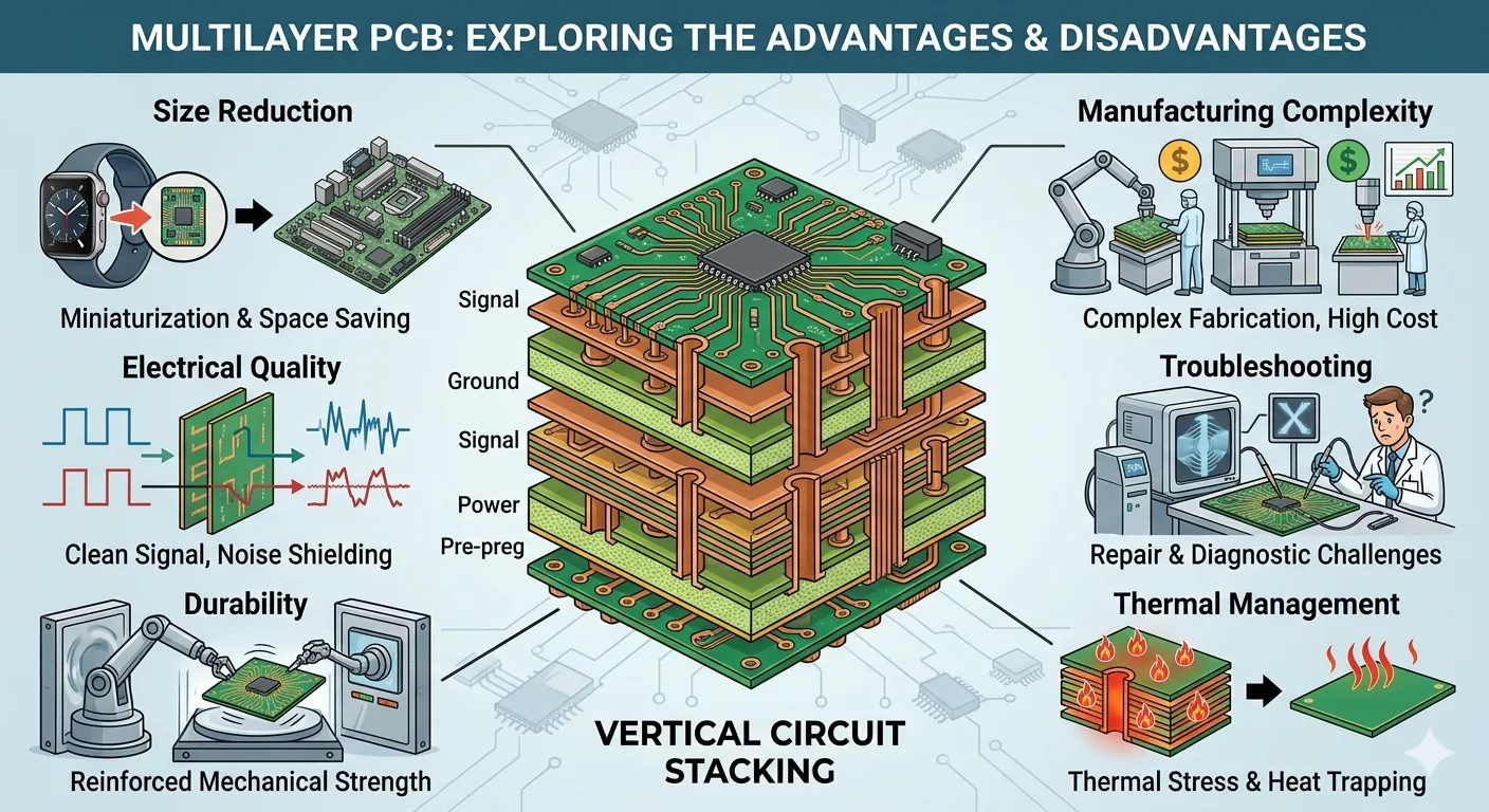
At its core, a Multilayer PCB consists of at least three layers of conductive copper foil. These layers are stacked and bonded together with layers of insulating material, known as prepreg or core, in between. This arrangement is far more sophisticated than a simple board. Because the circuits can run on internal layers, designers have much more room for components on the surface. They can also use "vias" to connect these different layers, acting like elevators for electrical signals. This vertical integration is the key to density. It allows for the routing of hundreds or even thousands of signals in a very compact footprint. Without this layering, our advanced electronics would be too bulky to fit into the sleek enclosures we use daily.
The Driving Force Behind Smartphones and Mobile Tech
The smartphone is perhaps the most impressive example of how we utilize the Multilayer PCB in our daily lives. A flagship phone is a dense concentration of hardware. It needs to fit a high-speed processor, memory modules, radio frequency antennas, and power management chips into a tiny, thin frame. If you were to look at the main board of a phone, you would see a complex, high-layer-count board. This allows engineers to route high-speed data signals between the processor and memory without them interfering with one another. It also ensures that the radio signals for 5G, Wi-Fi, and Bluetooth have dedicated ground planes to minimize noise. Every millimeter saved by using a multilayer board contributes to the phone being thinner and more powerful.
Revolutionizing High-Performance Computing
In the world of servers, workstations, and high-end laptops, the demand for processing power is constant. These systems perform trillions of calculations every second. This requires a board that can handle very high data speeds and significant power consumption. A Multilayer PCB is essential here because it allows for excellent signal integrity. Engineers can dedicate specific internal layers to ground and power, which provides a clean electrical environment for the fast-switching signals on the surface. This reduces the risk of data errors and system crashes. As we see a massive shift toward artificial intelligence and machine learning, the performance demands on these boards are only going to increase.
Advancements in Aerospace and Military Hardware
Aerospace and defense systems represent the absolute peak of engineering requirements. A board used in an avionics suite or a missile guidance system must survive the most extreme conditions imaginable. It must function perfectly under high vibration, extreme temperature shifts, and intense electromagnetic interference. The high-layer count of a Multilayer PCB allows for a redundant and robust design. Designers can build in multiple levels of safety and shielding to protect the signals from corruption. This level of reliability is non-negotiable when a failure could lead to catastrophic results. These boards are built with the highest quality materials and are tested to the most rigorous standards in the industry.
The Role of Multilayer PCB in Medical Equipment
Medical devices are increasingly becoming portable and highly intelligent. Think about modern handheld ultrasound machines, patient monitors, and even robotic surgical assistants. These devices must be reliable, compact, and precise. A Multilayer PCB allows for the integration of complex sensor data acquisition and signal processing on a single, small board. By keeping the signal path short and clean, the device can provide more accurate readings to the doctor or surgeon. This is a clear case where the sophistication of the board directly supports better patient outcomes. The miniaturization enabled by multilayer technology has moved life-saving technology from the hospital wall to the patient's bedside.
Powering Industrial Automation and Smart Factories
Factories are no longer just machines and gears; they are intelligent, connected ecosystems. Industrial robots, programmable logic controllers, and automated inspection systems are all built on robust electronics. These systems operate in harsh environments where dust, heat, and vibration are common. A Multilayer PCB is ideal for these applications because it can integrate a large number of functions into a single, compact unit. It also offers excellent shielding properties to prevent electrical noise from the factory floor from disrupting the control signals. By using these boards, companies can build more agile and capable manufacturing lines that operate with higher efficiency and less downtime.
The Backbone of Modern Networking Infrastructure
The internet is built on a massive physical network of switches, routers, and server blades. These devices handle massive amounts of traffic at incredible speeds. To maintain this speed, the hardware must be incredibly well-designed. A Multilayer PCB is used to manage the complex, high-speed routing required for fiber-optic links and massive data backplanes. The designers must carefully control the impedance of every trace on the board to ensure the signal stays sharp and clear. If the board design fails to maintain this integrity, the network will experience dropped packets and slow speeds. As we move toward even faster networking standards, the complexity of these boards continues to grow.
Why Signal Integrity is the Key to Success
In a Multilayer PCB, signal integrity is everything. When signals move at high frequencies, they can easily bleed into neighboring traces, causing crosstalk. This is like trying to have a private conversation in a room filled with people shouting. Designers use the internal layers of the board to act as "shields" between signal traces. They place ground planes directly beneath high-speed signals to provide a clean return path for the current. By mastering this "layer stack-up," engineers can build devices that are both incredibly fast and stable. This is a level of mastery that separates good designs from truly world-class products.
The Challenges of Manufacturing Complexity
Manufacturing a board with twenty or thirty layers is no small feat. The process requires extreme precision and advanced equipment. Each layer must be perfectly aligned with the one beneath it, or the holes drilled through the board—the vias—will not connect correctly. This requires advanced laser-drilling and precise automated alignment systems. Furthermore, as the number of layers increases, the thickness of the board must also be carefully managed to fit into the device's enclosure. This is why design and manufacturing are so tightly linked. A good designer knows the capabilities of the factory and plans the board accordingly.
Trends in Multilayer PCB Design
Looking toward the future, the trend is toward even more integration. We are seeing the rise of "embedded" components, where things like capacitors and resistors are actually placed inside the layers of the board rather than on the surface. This allows for even more density and even better electrical performance. We are also seeing the increased use of artificial intelligence in the design process to optimize the routing of these complex boards. AI can find the most efficient path for thousands of signals in seconds, a task that would take a human engineer days or even weeks. These innovations are keeping the industry on a rapid pace of progress.
Designing for Manufacturability (DFM)
A crucial concept for anyone working with these boards is "Design for Manufacturability." This means that the designer must anticipate potential issues during the board's construction. For example, they must ensure there is enough space for the drilling and soldering processes. They should also consider the thermal properties of the board to ensure it won't warp during the reflow process. By following DFM best practices, companies can avoid costly mistakes and shorten their product development time. This collaborative effort between the design team and the manufacturing shop is a hallmark of successful high-tech companies.
Environmental Impact and Sustainability
Like the rest of the electronics industry, the production of these boards must account for environmental impacts. The chemical processes used to etch the copper and plate the holes require careful waste management. Many manufacturers are now adopting greener, closed-loop systems to reduce their water usage and chemical output. Furthermore, there is an increasing focus on the recyclability of the final product. As we look at the entire lifecycle of our devices, the focus on sustainable manufacturing is becoming a top priority. This is a global challenge that the industry is addressing with new standards and better technology.
The Human Factor in Board Design
It is easy to focus on the machines, but the heart of this industry is the human expertise involved. Skilled PCB designers, process engineers, and quality control technicians are the ones who make it all happen. They spend their careers studying how electrons move through different materials and how to handle the challenges of ever-increasing density. Every breakthrough in technology, from your smartphone to your laptop, is the result of thousands of hours of human ingenuity and problem-solving. It is a collaborative community that is truly building the future of our digital world.
The Intersection of Software and Hardware
It is important to remember that the board is only one part of the equation. The firmware and software that run on the board are what make the device "smart." A well-designed Multilayer PCB provides a stable foundation for this intelligence. When the software is optimized for the hardware's capabilities, the result is a product that is truly seamless and efficient. This integration of software and hardware is why our technology feels so intuitive and powerful today. We are building systems that are becoming more intelligent with every passing year.
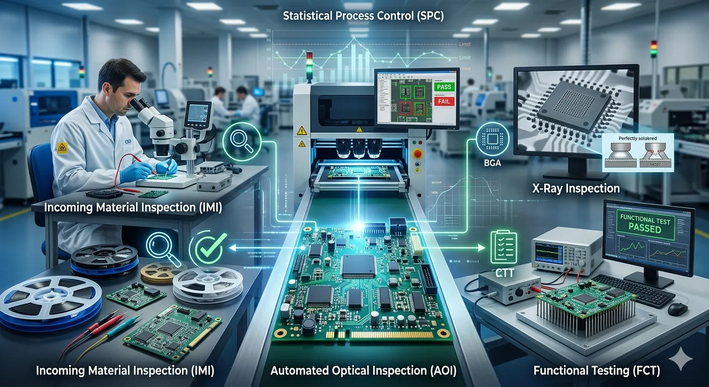
The Importance of Quality Assurance
Because these boards are used in so many critical applications, the quality assurance process is massive. Manufacturers use everything from X-ray machines to automated optical inspection to verify that every connection is perfect. A single bad solder joint on one of the inner layers could render the entire board useless. This is why testing is integrated into every step of the process. From the raw materials to the finished, populated board, the commitment to excellence is what makes our modern devices so incredibly reliable. It is the invisible guarantee that your device will work when you need it most.
Final Reflections on the Layered Future
The Multilayer PCB is a true marvel of modern engineering. It is the invisible force that enables the rapid pace of innovation we see in the consumer, industrial, and medical sectors. By stacking our technology, we have been able to achieve levels of performance that were once thought impossible. As we look ahead, we can expect this technology to continue to evolve. We will see faster speeds, smaller form factors, and even more efficient designs. Every time you pick up a smart device, take a moment to consider the complex, multi-layered world inside. It is one of the greatest accomplishments of our modern era.
Are you ready to optimize your next project with high-density board technology?
If your project requires more performance than a simple board can provide, it is time to explore the benefits of multilayer design. Don't let the limitations of legacy technology hold your innovation back. Partner with an expert manufacturer who understands the challenges of high-layer-count production. They can help you optimize your stack-up for the best possible signal integrity and manufacturing efficiency. Your design deserves a foundation as capable as your ideas. Reach out to a professional assembly and manufacturing partner today to see how you can take your next product to the next level of performance.


Sign in to leave a comment.