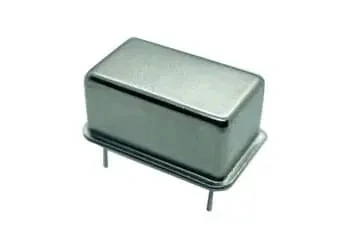
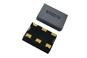
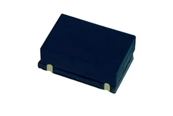
Specifications of SMD (12.6×20.2mm), Output CMOS, Sine Wave, Ultra Stable, Low Phase Noise OCXO
General Specifications:
Series: Ultra Stable, Low Phase Noise OCXO
Size: 12.6×20.2mm
Output Waveform: LVCMOS, Sine Wave
Features: High Frequency, Low Phase Noise
Dimensions: 12.6×20.2mm
Frequency Range: 10MHz~1450MHz
Jitter: 50fs
Frequency Pulling Range: ±25ppm, ±50ppm, ±100ppm
Output Wave: CMOS, LVDS, HCSL, LVPECL
Key Features:
Ultra Stable: Ensures minimal frequency deviation over time and temperature variations.
Low Phase Noise: Ideal for applications requiring high signal integrity.
High Frequency: Suitable for a wide range of high-frequency applications.
SMD Package: Compact size (12.6×20.2mm) for easy integration into various systems.
Applications:
Low Phase Noise Signal Source: Provides a stable and low-noise signal for precision applications.
Wireless Communication System: Enhances the performance of wireless communication systems by providing a stable frequency reference.
Low Jitter RF Communication: Ensures minimal signal distortion in RF communication systems.
GNSS (Global Navigation Satellite System): Improves the accuracy and reliability of GNSS systems by providing a stable frequency reference.
Summary:
This SMD OCXO (sine wave crystal oscillator) is designed for applications requiring ultra-stable, low phase noise performance in a compact package. With a frequency range of 10MHz to 1450MHz and various output waveforms (CMOS, LVDS, HCSL, LVPECL), it is suitable for a wide range of high-frequency and precision applications, including wireless communication systems, low jitter RF communication, and GNSS. The device’s low jitter (50fs) and frequency pulling range (±25ppm, ±50ppm, ±100ppm) further enhance its suitability for demanding applications.
There are many electronic crystal manufacturers, but we are one of the best choices for you.


Sign in to leave a comment.