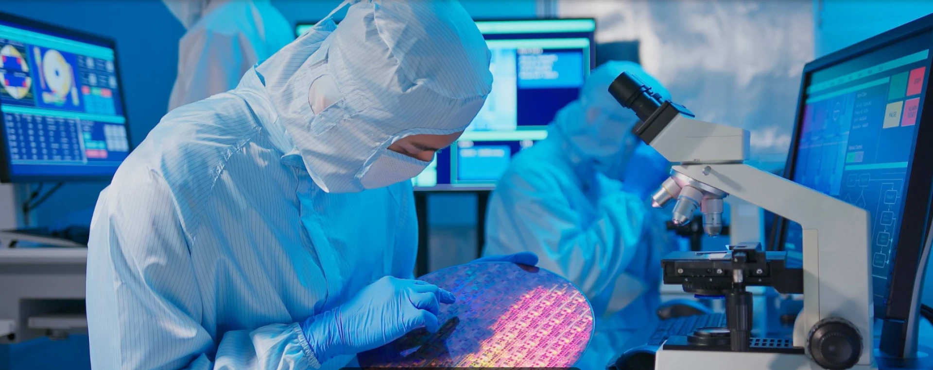
In the highly competitive field of electronics and chip manufacturing, accuracy is crucial. Semiconductors are tiny parts that are essential to every computer, smartphone, and automobile. These small brains must pass stringent electrical testing to guarantee flawless operation before they are packed and sold. This critical step is performed by specialized machines known as advanced semiconductor probers.
For decades, these probers have been essential. Still, the process has been truly revolutionized by two key areas: intelligent prober control software that manages the machine, and sophisticated probing peripherals that enable new types of tests. This combination has transformed testing from a manual, time-consuming effort into a seamless, automated process, significantly boosting quality and speed in modern production line environments.
This article breaks down how this new era of automation, driven by cutting-edge control systems and clever accessories, is redefining the future of device manufacturing.
Control software suites are the cornerstone of automation.
The brain of any modern testing system is its testing software. This software is far more than just a simple instruction manual; it is a sophisticated automation control platform that handles every micro-movement and measurement.
Defining the Control Platform
At its core, the control software serves as the interface between the human operator, the physical advanced semiconductor probers, and the external testing equipment for device testing. It dictates when and how the wafer moves, where the probes land, and what measurements are taken. It replaces the manual steps an operator would take, ensuring the process is followed precisely, every single time.
This move to a digital interface is the key to enabling system-level automation. It allows manufacturers to set up complex tests once and run them thousands of times without human interference, which is necessary for the massive volumes seen in electronics production.
Core Capabilities of Modern Testing Software
Numerous elements of contemporary wafer probe control systems are designed to manage the complexity of today's semiconductor devices. Creating recipes and managing test sequences are two primary tasks. An engineer can easily create a detailed recipe for a particular chip design by defining several measurements, voltage applications, and thermal cycling steps. This recipe is then perfectly carried out by the software.
Another critical component is the data acquisition software. This feature instantly collects the massive amounts of data generated during electrical measurement—from tiny changes in current to signal response times—and logs it in real-time. This immediate feedback is crucial for the entire semiconductor fabrication process, enabling engineers to identify issues promptly. Without this integrated system software suite, the sheer volume of data from high-throughput testing would be impossible to manage efficiently.
Achieving Repeatability and Accuracy
By relying on a control application, manufacturers can achieve unprecedented levels of process repeatability. The machine performs the same delicate motions with nanometer-scale precision, avoiding the tiny differences in pressure or alignment that can ruin a test.
This consistency directly translates into improved measurement accuracy. The probe operation programs constantly check their own calibration and positioning systems. The exact and hygienic electrical contact between the probe tip and the chip pad is guaranteed by this sturdy management system. The automation control platform ensures that every test result is reliable by reducing this variability, which can be the difference between a product that performs well and one that fails in the field.
Essential Probing Peripherals and System Integration
While the software is the brain, the physical components that enable specialized tests are the hands. The ecosystem of probing peripherals—the accessories and supplementary tools—is what allows advanced semiconductor probers to test everything from a simple memory cell to a complex radio-frequency (RF) chip.
Categorizing Probing Accessories and Tools
Probing peripherals are no longer just simple needles. They are a complex array of hardware components designed for specific functions.
- Thermal Chucks: These system add-ons are temperature-controlled platforms that hold the wafer. They are essential test environment tools that enable engineers to perform stress testing by running the chip from extreme cold (cryogenic) to very high temperatures, simulating real-world conditions such as automotive engine bays or deep-space environments.
- Specialized Probes: The tiny needles themselves are a key area of innovation. Probing consumables include highly precise RF probes for high-frequency measurements, and High-Power probes needed for new materials like Silicon Carbide (SiC) used in electric vehicles, which require testing at thousands of volts.
Impact of Hardware Components on Test Environment
These additional pieces of equipment must be integrated to adequately describe the gadget. For example, ultra-low noise settings are necessary for testing a micro-electromechanical system (MEMS) sensor. In this case, auxiliary systems that remove external noise and vibration—such as vacuum chucks or specialised isolation enclosures—become essential hardware elements.
Achieving the required measurement accuracy often depends entirely on the quality and integration of the probing peripherals. The software and the hardware must work together. The system software suite receives real-time thermal data from the chuck. It adjusts the test sequence accordingly, ensuring that the test is executed only when the chip is at the exact specified temperature.
Seamless Hardware-Software Interface
The interaction between the software and hardware is where the real revolution is. The control program receives constant feedback from every piece of hardware in addition to commands. This integrated workflows capability ensures that if a probe tip breaks or a thermal reading drifts, the advanced semiconductor probers system can immediately pause the test, log the error, and even start a new procedure, minimizing downtime and protecting the delicate wafer.
This seamless interface is what makes automated test execution reliable enough for a mass production setting.
Driving Operational Efficiency and High-Throughput Testing
The combined power of sophisticated control software and integrated probing peripherals has completely changed the economics of semiconductor fabrication. The primary benefits are found in dramatically improved speed and efficiency across the entire production line environment.
The Shift to Hands-Free Operation
The ability to rely on the automation control platform means that testing is no longer limited to the operator's shift. This shift to hands-free operation is known as unattended testing. A technician can load a cassette of wafers at the end of the day, and the prober will perform automated test execution throughout the night, using its computerized measurement capabilities to work tirelessly and without error.
This immediately translates to higher output. High-throughput testing is achieved by minimizing the time spent on manual setup, alignment, and data transfer. The operating efficiency of the entire fab is immediately increased because every second saved on a single chip is multiplied over millions of devices.
Real-World Impact on Manufacturing
The most significant measurable result of this automation is the substantial reduction in test time. By eliminating human-speed steps, automated systems can complete an electrical characterization in a fraction of the time a manual system requires. This speed is critical for reducing manufacturing bottlenecks and achieving faster time-to-market.
Furthermore, advanced semiconductor probers play a crucial role in maximizing yield management. By testing every chip early—a process known as wafer-level testing—manufacturers can identify defective chips before incurring the expense of expensive packaging. The cost savings from preventing the packaging of a single "bad die" can quickly offset the initial investment in system-level automation.
Advanced Data Logging and Analysis
A massive benefit that is often overlooked is the quality of the data. The data acquisition software in the system software suite logs every parameter of every test with complete consistency. This provides vast and reliable datasets, crucial for quality assurance (QA).
Engineers use this high-quality data to perform detailed device characterization and identify subtle process flaws. For example, suppose data logging capabilities show that devices fail only at a specific thermal point. In that case, engineers can trace the issue back to a flaw in the wafer's material or an error in the fabrication process, allowing for targeted process improvements and improved future yield management.
Future Directions in Automated Device Characterization
The evolution of automated testing is far from complete. As advanced semiconductor probers continue to evolve, they are transitioning toward more intelligent, more adaptable systems capable of addressing the increasingly complex challenges presented by future chip designs.
Combining machine learning and artificial intelligence
The next frontier for testing software lies in using artificial intelligence (AI). AI-driven control applications can analyze the vast stream of test data in real-time to spot patterns that human operators and traditional algorithms might miss.
For instance, machine learning can optimize the test flow itself. If a device fails an early, simple test, the AI can skip the rest of the complex, time-consuming tests for that chip, accelerating the automated test execution process. These probe operation programs become increasingly smarter over time, resulting in continuous improvements in operational efficiency.
Evolving Demands of New Technologies
The materials and designs used in new chips—such as devices for quantum computing, spintronic logic, or complex photonic components—require entirely new ways of probing. This is driving innovation in probing peripherals and auxiliary systems.
Test environment tools now often include cryogenic stages for testing at temperatures near absolute zero or specialized shielding for ultra-low-noise measurements. The probe control program must be flexible enough to integrate these new, often custom, hardware components, ensuring that the precision and performance needed for cutting-edge device characterization are met.
Summary of Advantages
The revolution in automated testing is a story of harmony between innovative software and sophisticated hardware. The advanced semiconductor probers available today, powered by powerful automation control platforms and supported by specialized probing peripherals, have moved beyond simple testing.


Sign in to leave a comment.