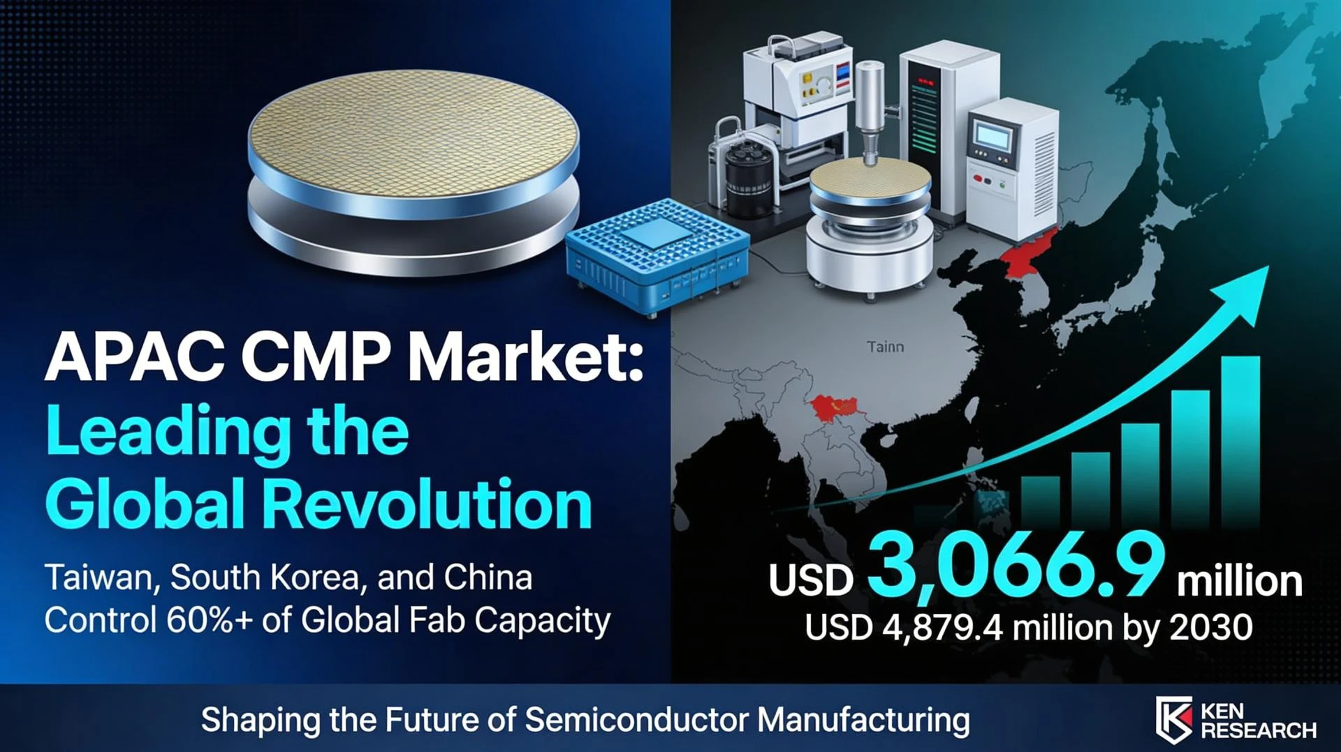
Three countries account for the overwhelming majority of the world's active semiconductor fabrication capacity and all three are in Asia Pacific. Taiwan holds approximately 44% of global foundry capacity as of 2024, followed by China at 28% and South Korea at 12% a combined share that makes APAC the undisputed centre of global chip production. Every wafer start across those fabs is a direct chemical mechanical planarization demand event: more CMP equipment utilised, more consumables consumed, more precision process steps required per die. The result is an APAC CMP market that generated USD 3,066.9 million in 2024, accounting for 48% of global CMP revenue, and is forecast to reach USD 4,879.4 million by 2030 at a CAGR of 8%.
The Asia Pacific Chemical Mechanical Planarization Market by Ken Research maps the full demand picture how fab concentration across these three economies translates into CMP equipment and consumables spend, which application segments are driving volume, and how the competitive landscape is positioned through 2030. Ken Research provides the complete market size, segment, and country-level analytical framework this blog draws from.
How Fab Concentration in Three Countries Creates a Self-Reinforcing CMP Demand Base
Fab concentration does not just correlate with CMP demand it mechanically produces it. Every additional wafer start in an advanced fab requires multiple planarization passes, and every node transition multiplies the number of those passes per wafer. Taiwan, South Korea, and China's combined dominance of global fab capacity means that the structural floor for APAC CMP demand is wide and widening.
Taiwan: Advanced Node Volume and the Foundry Effect on CMP Intensity
Taiwan's foundry leadership is inseparable from CMP demand intensity. Leading-edge logic production at advanced nodes sub-5nm and the emerging Gate-All-Around (GAA) architecture requires a significantly higher number of CMP process steps per wafer than mature nodes. Leading-edge capacity for 5nm nodes and under is expected to grow 13% in 2024, chiefly driven by generative AI for data centre training, inference, and leading-edge devices, with GAA chip production set to boost total leading-edge capacity growth by 17% in 2025. Each incremental wafer at these nodes is a disproportionately large CMP demand event compared to a mature-node wafer compounding both equipment utilisation and specialised slurry consumption.
South Korea: Memory-Driven CMP Demand and the HBM Multiplier
South Korea's CMP demand profile is shaped by its dominance in DRAM and 3D NAND memory production. High-Bandwidth Memory (HBM) the memory architecture powering AI accelerator chips involves through-silicon via (TSV) processes that require precision CMP steps at every die layer within the stack. As documented in the APAC CMP market CAGR analysis by Ken Research, memory is a structurally important and growing application driver within the APAC market and HBM's expansion is adding a layer of consumable intensity per stack that did not exist at the scale of previous memory generations. DRAM capacity is expected to increase by 9% in both 2024 and 2025, driven by the expansion of AI to edge devices.
China: Mature-Node Scale and the Volume CMP Equation
China's contribution to APAC CMP demand operates on a different logic from Taiwan and South Korea. Rather than advanced node intensity, it is raw volume at mature nodes that drives demand. China's fab capacity reached 8.85 million wafers per month in 2024 and is projected to grow a further 14% to 10.1 million wpm in 2025 nearly a third of the global total. At that scale, even mature-node CMP consumption generates enormous recurring demand for polishing pads, slurries, and pad conditioners. As noted in the Asia Pacific chemical mechanical planarization market report by Ken Research, China's capacity expansion government-backed and sustained is a structural pillar of the region's CMP consumables base through 2030.
What Three-Country Fab Dominance Means for CMP Equipment and Consumables Segments
The fab concentration dynamic plays out differently across the two primary CMP market segments equipment and consumables creating distinct but reinforcing demand patterns that underpin the market's 8% CAGR through 2030.
CMP Equipment Largest and Fastest-Growing Segment: Equipment spend is front-loaded into fab construction and node transitions. As fabs across Taiwan, South Korea, and China invest in advanced node production and capacity expansion, they procure new-generation CMP polishing and grinding systems capable of meeting the tighter uniformity tolerances of sub-5nm and GAA architectures. Ken Research identifies CMP equipment as both the largest revenue segment and the fastest-growing segment in the APAC market through 2030 a dual status that directly reflects the active fab investment wave across all three countries simultaneously.
CMP Consumables Recurring Revenue at Scale: Slurries, polishing pads, and pad conditioners are consumed per wafer start, scaling proportionally with every fab's production output regardless of whether new equipment has been purchased. The breadth of the APAC consumables base is expanding beyond silicon oxide slurries into specialised formulations for copper, tungsten, and barrier-layer applications at advanced nodes and into tailored chemistries for compound semiconductors and MEMS devices. As documented in the CMP consumables market Asia Pacific analysis by Ken Research, this broadening formulation complexity is widening the consumables revenue base beyond volume growth alone. The upstream context for this trajectory is provided by the Asia-Pacific Semiconductor Market analysis by Ken Research, valued at USD 324 billion in 2023, which demonstrates the scale of semiconductor output that consumable replenishment cycles serve.
HBM and Advanced Packaging The Emerging CMP Intensity Layer: Beyond conventional IC and memory fabrication, advanced packaging technologies including 3D ICs, heterogeneous integration, and HBM stacks are introducing additional CMP requirements at the back-end of the production process. South Korea's leading memory producers and Taiwan's advanced packaging operations are both contributing to this emerging layer of CMP demand, which sits on top of front-end wafer fabrication and amplifies the overall addressable market. The Global High Bandwidth Memory Market report by Ken Research, valued at USD 3.5 billion, provides the context for how HBM production growth in South Korea and Taiwan is feeding directly into incremental CMP demand.
If you want country-level CMP demand breakdowns, segment-level revenue forecasts, and the full competitive landscape across APAC through 2030, download free sample for a detailed preview of the full market analysis.
Conclusion
The link between Taiwan, South Korea, and China's combined control of 60%+ of global fab capacity and APAC's 48% share of global CMP revenue is not coincidental it is mechanical. More fabs, more wafer starts, more advanced nodes, more planarization steps. The CMP equipment segment is benefiting from the front-loaded fab investment wave; the consumables segment is benefiting from the compounding production volume those fabs generate. Neither dynamic is cyclical both are structural, extending through 2030 and reinforced by policy-backed capacity expansion programs across all three economies. India's emergence as a growing fab destination adds a further incremental layer to the APAC CMP demand base beyond the forecast period.
For suppliers, investors, and strategists building positions in the APAC semiconductor supply chain, the full analytical picture segment-level forecasts, country data, player dynamics, and the Asia Pacific CMP competitive landscape is documented in the Asia Pacific Chemical Mechanical Planarization Market Outlook to 2030 by Ken Research.
Frequently Asked Questions
Why does APAC dominate the global CMP market?
According to Ken Research, APAC dominates the global chemical mechanical planarization market because Taiwan, South Korea, and China collectively account for over 60% of global semiconductor fab capacity. Every wafer start in those fabs requires multiple CMP process steps making APAC's fab concentration the direct structural driver of its 48% share of global CMP revenue in 2024.
What is driving CMP market growth in Asia Pacific through 2030?
Ken Research highlights that APAC CMP growth at a CAGR of 8% to 2030 is driven by advanced node transitions multiplying planarization steps per wafer, China's expanding mature-node fab capacity, South Korea's HBM and DRAM production growth, and government-backed semiconductor investment programmes across Taiwan, Japan, and India extending the region's output lead through the forecast period.
Which CMP segment is growing fastest in Asia Pacific?
As per the Asia Pacific Chemical Mechanical Planarization Market Outlook by Ken Research, CMP equipment is both the largest revenue segment and the fastest-growing segment in the APAC market through 2030. Equipment demand is front-loaded into fab builds and node transitions, with new-generation polishing systems required to meet the tighter uniformity tolerances of sub-5nm and Gate-All-Around architectures being deployed across APAC fabs.
How does HBM production affect CMP demand in South Korea?
Ken Research's market analysis reveals that High-Bandwidth Memory (HBM) production which involves through-silicon via (TSV) stacking processes requires precision CMP steps at each die layer within the stack. As South Korea's leading memory producers scale HBM output for AI accelerator applications, the number of CMP operations per finished package increases significantly, creating an additional layer of consumable intensity on top of conventional memory fab demand.


Sign in to leave a comment.