A bare board and the bare board testing procedure play key roles in the manufacturing of a printed circuit board (PCB). The bare board layout specifies the location of through holes and electronic components in PCB development. This PCB substrate also determines the connections of a finished board via its printed circuitry. You can increase the dependability of your results by incorporating bare board testing into your PCB creation process.
WHAT EXACTLY IS A BARE BOARD?
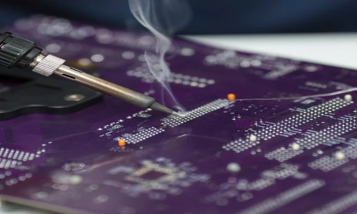
The term "bare board" in PCB terminology refers to the state of a PCB before it receives electronic components or through holes. The PCB substrate, metal covering, electrical channels, and designs comprise a bare board. A bare board is referred to as a PCB by some industry professionals, while an assembled board is referred to as a PCBA.
WHAT EXACTLY IS BARE BOARD TESTING?
The continuity and isolation of a bare circuit board's connections are tested during bare board testing. The continuity testing processes verify that there are no open places in the circuits that will hinder current flow. Isolation testing, on the other hand, examines the resistance between two distinct electrical connections.
To undertake bare board testing, PCB makers employ one of two methods:
Pinned fixture test: Spring-loaded pogo pins test all of the board's connecting surfaces simultaneously during a pinned fixture test. To ensure a connection throughout the PCB, top and bottom plates apply pressure to a bespoke pin fixture. This method, which can test thousands of sites at once, is more efficient than the flying probe test. The test takes around five seconds to complete after the individual testing the board sets up the pogo pins.
Flying probe test: The flying probe test for bare boards employs two robotic arms outfitted with poles to examine the connections on a PCB. These flying probes follow instructions from a software program to traverse the connections. In exchange for longer testing lengths, the flying probe approach is less expensive and more flexible than the pinned fixture test. It is appropriate for smaller production volumes where slower testing speeds will not interfere with the design process.
THE ADVANTAGES OF BARE BOARD TESTING
Incorporating bare board testing into the PCB design process can result in:
Savings: Extensive testing during the early phases of design will help you save money on the costs associated with improperly built PCBs.
Streamlined production: Production can be streamlined by recognizing flaws during the prototyping stage and saving time in subsequent stages of production.
Issue resolution: Bare board testing will assist you in identifying potential issues early in production while narrowing the cause of each problem.
WHEN SHOULD YOU USE BARE BOARD TESTING FOR YOUR PCB?
In most cases, this form of assessment can help you optimize the PCB design process. Bare board testing is particularly valuable in the early stages of development, when it can save the most money and time. By incorporating bare board testing from the start, you may streamline many elements of production.
PCB Power and small-scale manufacturing services when you need a PCB supplier to fit your testing methods. Request a quote now to learn more about our capabilities.
Original source: https://ibusinessday.com/when-should-i-use-bare-board-testing/


Sign in to leave a comment.