For many years, blade dicing has been the preferred singulation process for thin and ultrathin silicon wafers. The method is characterized by high speed, low damage and small kerf width.
However, blade dicing has several limitations. For example, edge chipping and blade wear can reduce yields and cause burring, which could damage the die.
High Precision
Laser dicing is a process that uses a laser to cut dies from silicon wafers. These dies are the basis for many electronics, including semiconductors and microchips.
The laser dicing process has a number of benefits, including high precision and high throughput. It also reduces the need for expensive machining tools and allows for more efficient processing.
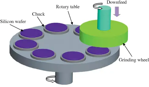
Dicing is a highly automated process that involves cutting precise dies from silicon wafers. These cut patterns are then used to create printed circuit boards or other electronic devices.
There are several different types of dicing methods that use lasers for the process. One method, called laser ablation dicing, uses a laser to heat the surface of the wafer and create a cut pattern as needed. Cooling water is then added to protect the wafer from thermal damage.
A third dicing process, known as laser full cut dicing, uses a laser to remove the layer of wire insulation that is usually attached to the backside of thinned wafers, such as those used in high-speed logic applications. This can eliminate the risk of peeling and breakage that occurs during traditional blade dicing.
High Throughput
With increasing complexity in semiconductor devices, wafer fabs are facing the challenge of reducing costs and improving yields. The technology is also constantly evolving with new materials, die attach films and tinier chips that require increasingly complicated manufacturing processes.
Laser dicing, on the other hand, uses lasers instead of blades to cut wafers at high speed in a dry process. This dry process prevents contaminating dust particles and the cutting blade from contacting the wafer.
During laser dicing, water or another cooling agent sprays along the cutting lines to control the temperature of the substrate. The cooling agent also protects the wafer from thermal damage and particle contamination while the blade cuts through it.
The dicing machine then moves the blade to the next part of the wafer and repeats the process until all the wafers have been sliced. Once the dicing process is complete, the wafers are placed on a dicing tape and frame for further processing in the electronics assembly.
In order to address this issue, researchers at CUHK developed a laser-based process for dicing silicon wafers. The process utilizes multiple Bessel beams to perform the dicing operation in parallel, achieving higher throughput with both nanosecond and femtosecond lasers.
Reduced Particle Generation
With the semiconductor industry pushing towards thinner die, and increasing demands for higher performance with less power loss, laser dicing San Jose has become an integral part of manufacturing. This enables faster processing, improved accuracy and utilization of material, as well as minimal particle generation that allows for the production of more complex, dies with increased quality.
There are two major types of laser dicing: blade dicing and ablation dicing. Blade dicing uses a blade saw to cut wafers, while ablation dicing utilizes a laser to vaporize, sublime and remove material from a wafer.
Both methods can be effective on some devices. However, both methods have their limitations and can result in a lower yield than other dicing techniques. The main difference is that the blade dicing method causes chipping, debris and delamination while the ablation dicing method does not.
The primary reason for this is that the blade dicing process is mechanical, while the ablation dicing process is non-contact. This means that the laser beam is not subject to vibration or damage from the mechanical stress of the blade.
Ultimately, the choice between laser dicing and blade dicing comes down to the type of device being diced. Blade dicing is typically used on robust devices, while ablation dicing is more common for softer devices. For these reasons, it is important to choose a dicing technique that will be appropriate for the application.
Lower Costs
Laser Dicing is Changing the Game in Manufacturing
One of the biggest reasons why laser icing is changing the game in manufacturing is its ability to lower costs. It can be especially beneficial to manufacturers who use a lot of metals or other materials that have varying levels of thickness. This can result in a difference in the quality of the edges produced by the laser and the efficiency of the beam.
However, if you optimize your design file for laser cutting, you can actually save a significant amount of money. Think of it like a jigsaw puzzle: If you break the pieces up into smaller, more manageable pieces, they will take less time to put together.
Similarly, if you make your design file easier for the machine to read, it will cut much faster, which can also help lower your costs. That's why it's important to keep your design files as simple and efficient as possible.
To get started, you'll need to upload a design file and choose your material. You can use a free, online tool to do this.
In addition to this, it's also important to remember that a thicker or lighter material will also affect how fast the machine can cut. This can also lead to a decrease in the costs of the cut, as thin and light materials are less expensive to produce than heavier materials.
This can be especially important if you're using a laser dicing process to manufacture complex chip designs. For example, if you're producing micro-electro-mechanical systems (MEMS) and want to produce ultra-smooth surfaces on your chips, you'll need to choose a thinner wafer that will allow the laser to easily reach the surface of each die.
Thanks for visiting writeupcafe