Nanotechnology focuses on materials at the scale of atoms and molecules—typically between 1 and 100 nanometers. At this level, materials behave very differently from their bulk counterparts, showing unique electrical, optical, mechanical, and chemical properties. To understand and control these behaviors, scientists depend on precise characterization tools. One of the most powerful and widely used techniques is the X-Ray Diffractometer (XRD).
This detailed guide explains how XRD is used in nanotechnology to measure crystallite size and analyze crystal structure, along with its principles, applications, advantages, and limitations.
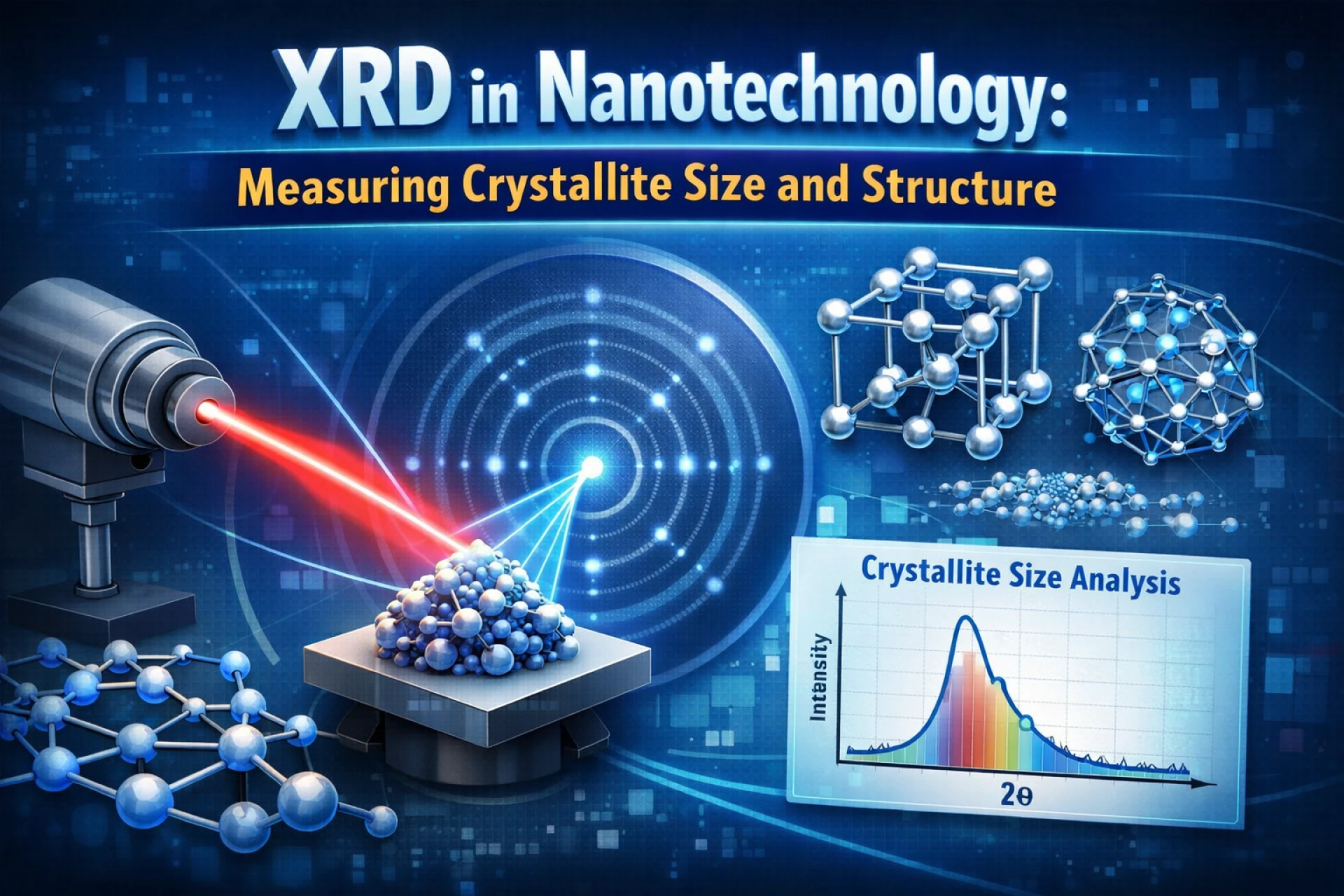
Introduction to XRD in Nanotechnology
An X-Ray Diffractometer (XRD) is an analytical instrument that helps determine the atomic and molecular structure of a material. It works by directing X-rays onto a sample and analyzing how those rays are diffracted.
In nanotechnology, XRD is especially important because:
- Nanomaterials often have very small crystalline domains (crystallites)
- Structural changes at the nanoscale directly affect material performance
- Accurate measurement of size and structure is critical for research and industrial applications
Unlike conventional materials, nanomaterials often exhibit peak broadening and shifts in XRD patterns, which provide valuable information about their size and internal structure.
Working Principle of XRD
The operation of XRD is based on Bragg’s Law, which explains how X-rays interact with the crystal lattice of a material.
When a beam of X-rays strikes a crystalline sample:
- The atoms in the crystal scatter the X-rays in different directions
- At certain angles, these scattered waves interfere constructively
- This produces a diffraction pattern consisting of peaks
Each peak corresponds to a specific set of atomic planes within the crystal. By analyzing these peaks, scientists can determine:
- The arrangement of atoms
- The spacing between crystal planes
- The overall structure of the material
In nanomaterials, the diffraction peaks are often broader and less intense compared to bulk materials, and this is a key feature used for size analysis.
Measuring Crystallite Size Using XRD
One of the most important applications of XRD in nanotechnology is determining crystallite size. A crystallite is a small, coherent crystalline domain within a material. It is important to note that crystallite size is not always the same as particle size—particles may consist of multiple crystallites.
The Scherrer Equation
Crystallite size is commonly estimated using the Scherrer Equation, which relates peak broadening in the diffraction pattern to the size of the crystallites.
Key idea:
- Smaller crystallites cause broader diffraction peaks
- Larger crystallites produce sharper peaks
Why Peak Broadening Occurs
In nanomaterials:
- The number of repeating atomic planes is limited
- This causes uncertainty in diffraction conditions
- As a result, peaks become wider
By measuring the width of these peaks, scientists can estimate the average crystallite size, often in the nanometer range.
Structural Analysis of Nanomaterials Using XRD
Beyond size measurement, XRD provides detailed insights into the internal structure of nanomaterials.
1. Phase Identification
Each material has a unique diffraction pattern. By comparing the obtained pattern with reference databases, researchers can identify:
- Different phases present in the sample
- Impurities or secondary materials
This is crucial in nanotechnology, where even small impurities can significantly affect performance.
2. Crystal Structure Determination
XRD reveals the arrangement of atoms within a material, such as:
- Cubic
- Tetragonal
- Hexagonal structures
Understanding the crystal structure helps predict material properties like strength, conductivity, and reactivity.
3. Lattice Parameters
XRD can calculate the dimensions of the unit cell (the smallest repeating unit in a crystal). In nanomaterials:
- Lattice parameters may change due to strain
- Surface effects can distort atomic spacing
These variations are important for designing advanced materials.
4. Crystallinity Assessment
XRD distinguishes between:
- Crystalline materials (sharp, well-defined peaks)
- Amorphous materials (broad, diffuse patterns)
Nanomaterials often contain both crystalline and amorphous regions, and XRD helps quantify their proportions.
5. Strain and Defect Analysis
Peak shifts and additional broadening can indicate:
- Internal stress
- Lattice strain
- Structural defects
These factors are critical in nanotechnology because they directly influence material behavior.
Applications of XRD in Nanotechnology
XRD is used across a wide range of nanotechnology applications:
🔹 Nanoparticle Characterization
- Measuring crystallite size of nanoparticles
- Identifying phases in nanocomposites
- Studying metal oxides like ZnO and TiO₂
🔹 Semiconductor Industry
- Analyzing thin films and nanostructures
- Ensuring crystal quality in electronic devices
🔹 Pharmaceuticals
- Studying drug crystallinity at nanoscale
- Improving solubility and bioavailability
🔹 Energy Materials
- Evaluating nanomaterials in batteries and solar cells
- Studying catalysts and fuel cell components
🔹 Environmental Science
- Analyzing nanomaterials used in water purification
- Studying adsorption and catalytic behavior
Limitations of XRD in Nanotechnology
Despite its advantages, XRD has some limitations:
- It measures crystallite size, not actual particle size
- It requires the material to be crystalline
- Overlapping peaks can make interpretation difficult
- It may not detect very small amounts of amorphous content
Because of these limitations, XRD is often used alongside other techniques such as electron microscopy for a complete analysis.
Best Practices for Accurate Results
To obtain reliable XRD data in nanotechnology:
- Prepare samples carefully (fine, uniform powder)
- Avoid contamination or moisture
- Use proper calibration standards
- Optimize instrument settings
- Combine XRD with complementary methods for validation
Future Trends in XRD for Nanotechnology
XRD technology continues to evolve, making it even more powerful for nanoscale research:
- High-resolution XRD for precise structural analysis
- In-situ XRD for studying materials under real conditions
- Synchrotron radiation sources for ultra-fast measurements
- AI-based data analysis for faster and more accurate interpretation
These advancements are helping scientists push the boundaries of nanotechnology.
Conclusion
X-Ray Diffractometry is an essential tool in nanotechnology for measuring crystallite size and understanding crystal structure. By analyzing diffraction patterns and applying principles like Bragg’s Law and the Scherrer Equation, researchers can gain deep insights into material properties at the nanoscale.
Whether in research laboratories or industrial applications, XRD continues to play a critical role in developing advanced materials that power modern technologies.


Sign in to leave a comment.